How to Use 24LC256: Examples, Pinouts, and Specs

24LC256 EEPROM Documentation
1. Introduction
The 24LC256 is a 256 Kbit (32K x 8) Electrically Erasable Programmable Read-Only Memory (EEPROM) manufactured by Anyone. It is designed for non-volatile data storage, meaning it retains data even when power is removed. The 24LC256 communicates using the I2C (Inter-Integrated Circuit) protocol, making it easy to interface with microcontrollers such as the Arduino UNO.
Common Applications:
- Data logging and storage
- Configuration data storage
- Calibration data retention
- Storing lookup tables or user-defined settings
- Embedded systems requiring non-volatile memory
The 24LC256 is widely used in applications where reliable, long-term data storage is required, and its I2C interface ensures compatibility with a variety of microcontrollers and systems.
2. Technical Specifications
The following table outlines the key technical details of the 24LC256:
| Parameter | Value |
|---|---|
| Memory Size | 256 Kbit (32K x 8) |
| Interface | I2C (2-wire) |
| Operating Voltage Range | 2.5V to 5.5V |
| Maximum Clock Frequency | 400 kHz (Fast Mode I2C) |
| Write Cycle Time | 5 ms (typical) |
| Data Retention | > 200 years |
| Endurance | 1,000,000 write/erase cycles |
| Operating Temperature | -40°C to +85°C |
| Package Options | PDIP, SOIC, TSSOP, MSOP |
Pin Configuration and Descriptions
The 24LC256 is typically available in an 8-pin package. The pinout and descriptions are as follows:
| Pin Number | Pin Name | Description |
|---|---|---|
| 1 | A0 | Address input bit 0 (used for I2C slave address selection) |
| 2 | A1 | Address input bit 1 (used for I2C slave address selection) |
| 3 | A2 | Address input bit 2 (used for I2C slave address selection) |
| 4 | VSS | Ground (0V reference) |
| 5 | SDA | Serial Data (I2C data line, open-drain) |
| 6 | SCL | Serial Clock (I2C clock line, open-drain) |
| 7 | WP | Write Protect (active HIGH, disables write operations when HIGH) |
| 8 | VCC | Power supply (2.5V to 5.5V) |
3. Usage Instructions
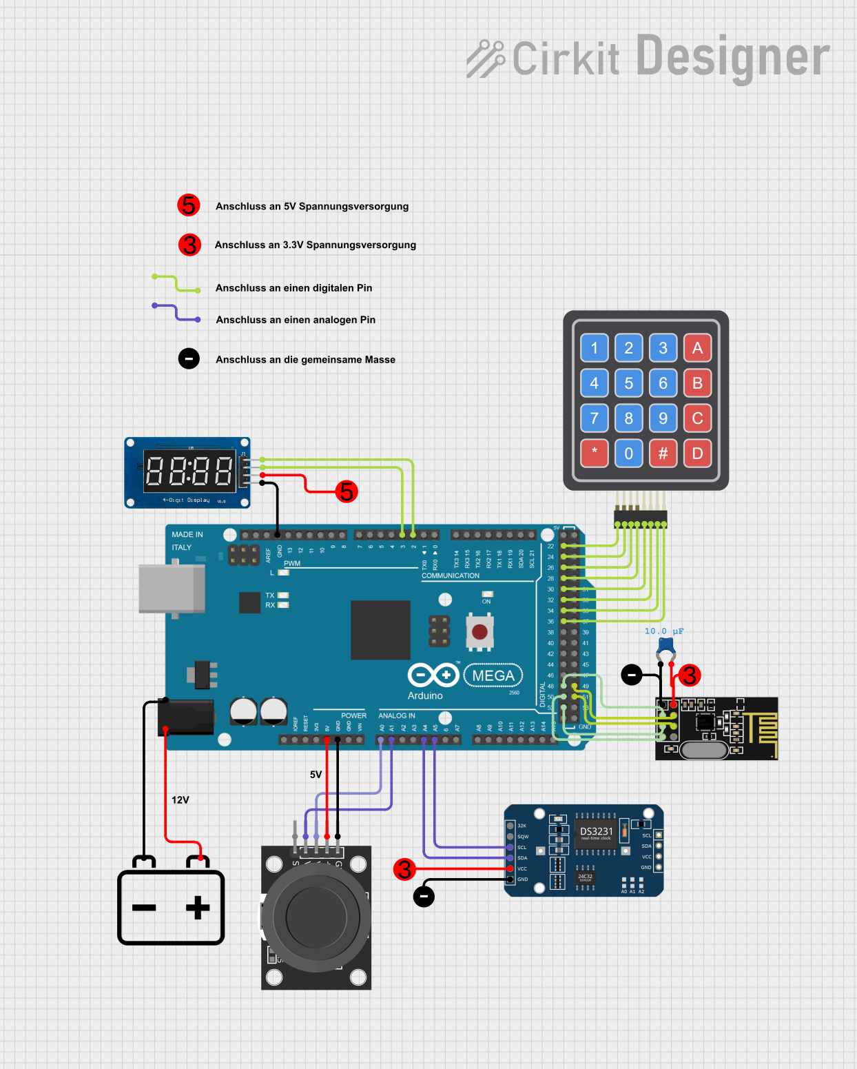
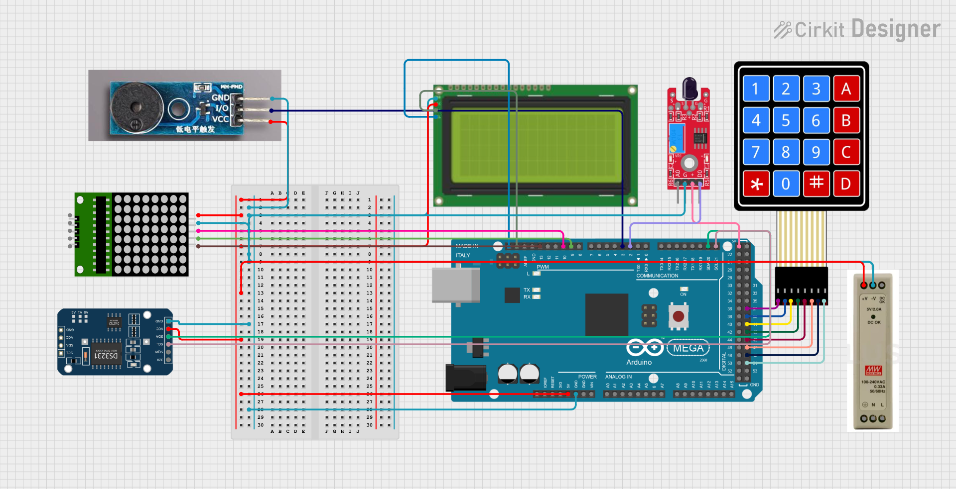
Connecting the 24LC256 to an Arduino UNO
To use the 24LC256 with an Arduino UNO, connect the pins as follows:
| 24LC256 Pin | Arduino UNO Pin | Description |
|---|---|---|
| VCC | 5V | Power supply |
| VSS | GND | Ground |
| SDA | A4 | I2C data line |
| SCL | A5 | I2C clock line |
| WP | GND | Disable write protection |
| A0, A1, A2 | GND or VCC | Set I2C slave address (see below) |
I2C Address Selection
The 24LC256 allows for up to 8 devices to be connected on the same I2C bus. The I2C slave address is determined by the states of the A0, A1, and A2 pins:
| A2 | A1 | A0 | I2C Address |
|---|---|---|---|
| 0 | 0 | 0 | 0x50 |
| 0 | 0 | 1 | 0x51 |
| 0 | 1 | 0 | 0x52 |
| 0 | 1 | 1 | 0x53 |
| 1 | 0 | 0 | 0x54 |
| 1 | 0 | 1 | 0x55 |
| 1 | 1 | 0 | 0x56 |
| 1 | 1 | 1 | 0x57 |
Example Arduino Code
Below is an example of how to write and read data from the 24LC256 using an Arduino UNO:
#include <Wire.h> // Include the Wire library for I2C communication

#define EEPROM_I2C_ADDRESS 0x50 // Base I2C address of the 24LC256

void setup() {
  Wire.begin(); // Initialize I2C communication
  Serial.begin(9600); // Initialize serial communication for debugging
  writeEEPROM(0x0000, 42); // Write the value 42 to memory address 0x0000
  delay(10); // Wait for the write cycle to complete
  int value = readEEPROM(0x0000); // Read the value from memory address 0x0000
  Serial.print("Read value: ");
  Serial.println(value); // Print the read value to the Serial Monitor
}

void loop() {
  // Main loop does nothing in this example
}

// Function to write a byte to the 24LC256
void writeEEPROM(unsigned int address, byte data) {
  Wire.beginTransmission(EEPROM_I2C_ADDRESS);
  Wire.write((address >> 8) & 0xFF); // Send the high byte of the address
  Wire.write(address & 0xFF);        // Send the low byte of the address
  Wire.write(data);                  // Send the data byte
  Wire.endTransmission();            // End the I2C transmission
  delay(5); // Wait for the write cycle to complete (typical 5ms)
}

// Function to read a byte from the 24LC256
byte readEEPROM(unsigned int address) {
  Wire.beginTransmission(EEPROM_I2C_ADDRESS);
  Wire.write((address >> 8) & 0xFF); // Send the high byte of the address
  Wire.write(address & 0xFF);        // Send the low byte of the address
  Wire.endTransmission();            // End the I2C transmission
  Wire.requestFrom(EEPROM_I2C_ADDRESS, 1); // Request 1 byte from the EEPROM
  if (Wire.available()) {
    return Wire.read(); // Return the received byte
  }
  return 0xFF; // Return 0xFF if no data is available
}
Best Practices
- Pull-up Resistors: Use 4.7kΩ pull-up resistors on the SDA and SCL lines for reliable I2C communication.
- Write Protection: Connect the WP pin to GND unless write protection is required.
- Address Management: Ensure unique I2C addresses when using multiple 24LC256 devices on the same bus.
- Write Delays: Always allow sufficient time (5ms) for write cycles to complete.
4. Troubleshooting and FAQs
Common Issues and Solutions
| Issue | Possible Cause | Solution |
|---|---|---|
| Cannot communicate with the EEPROM | Incorrect I2C address or wiring | Verify the A0, A1, A2 pin configuration and wiring. |
| Data not being written to the EEPROM | WP pin is HIGH (write protection enabled) | Connect the WP pin to GND to enable write operations. |
| Corrupted or incorrect data read | Insufficient delay after write operation | Add a delay of at least 5ms after each write operation. |
| EEPROM not detected on the I2C bus | Missing pull-up resistors on SDA/SCL lines | Add 4.7kΩ pull-up resistors to the SDA and SCL lines. |
FAQs
Can I use the 24LC256 with 3.3V systems?
- Yes, the 24LC256 operates within a voltage range of 2.5V to 5.5V, making it compatible with 3.3V systems.
How many write cycles can the 24LC256 handle?
- The 24LC256 is rated for 1,000,000 write/erase cycles per memory cell.
What happens if I exceed the memory size?
- Writing beyond the 32K memory size will wrap around to the beginning of the memory.
Can I use multiple 24LC256 chips on the same I2C bus?
- Yes, up to 8 devices can be used by configuring the A0, A1, and A2 pins for unique addresses.
This documentation provides a comprehensive guide to using the 24LC256 EEPROM
Explore Projects Built with 24LC256
Explore Projects Built with 24LC256