How to Use pcb_2: Examples, Pinouts, and Specs
Introduction
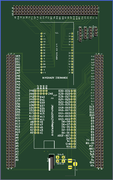
The PCB_2, manufactured by Νικολάου Νίκος (Part ID: Πλακέτα), is a high-quality printed circuit board designed for mounting electronic components. It provides both electrical connections and mechanical support, making it an essential component in electronic circuit design. The PCB_2 is versatile and suitable for a wide range of applications, from prototyping to industrial-grade electronics.
Explore Projects Built with pcb_2
Explore Projects Built with pcb_2
Common Applications and Use Cases
- Prototyping and development of electronic circuits
- Mounting and interconnecting components in consumer electronics
- Industrial control systems and automation
- Educational projects and DIY electronics
- Embedded systems and IoT devices
Technical Specifications
The PCB_2 is designed to meet the needs of both hobbyists and professionals. Below are its key technical specifications:
General Specifications
| Parameter | Value |
|---|---|
| Manufacturer | Νικολάου Νίκος |
| Part ID | Πλακέτα |
| Material | FR4 (Flame Retardant 4) |
| Layers | 2 |
| Board Thickness | 1.6 mm |
| Copper Thickness | 35 µm (1 oz/ft²) |
| Surface Finish | HASL (Hot Air Solder Leveling) |
| Solder Mask Color | Green |
| Silkscreen Color | White |
| Operating Temperature | -40°C to +85°C |
Electrical Specifications
| Parameter | Value |
|---|---|
| Maximum Voltage | 50 V |
| Maximum Current | 2 A per trace (depending on width) |
| Dielectric Constant | 4.5 |
| Insulation Resistance | >10⁶ MΩ |
Pin Configuration and Descriptions
The PCB_2 does not have predefined pins, as it is a customizable board for mounting components. However, it includes the following features:
- Through-Hole Pads: For mounting components with leads.
- Surface-Mount Pads: For SMD (Surface-Mount Device) components.
- Power and Ground Planes: Dedicated layers for power distribution and grounding.
- Vias: For interconnecting layers.
Usage Instructions
The PCB_2 is straightforward to use and can be adapted for various circuit designs. Follow these steps and best practices to ensure optimal performance:
How to Use the PCB_2 in a Circuit
Design the Circuit Layout:
- Use PCB design software (e.g., KiCad, Eagle, or Altium) to create the schematic and layout.
- Ensure proper trace width for current-carrying paths and adequate spacing between traces.
Prepare the PCB:
- Print the design onto the PCB_2 using a suitable fabrication method (e.g., etching or CNC milling).
- Apply solder mask and silkscreen if required.
Mount Components:
- Solder through-hole or surface-mount components onto the board.
- Use flux to ensure clean and reliable solder joints.
Test the Circuit:
- Verify connections using a multimeter.
- Power the circuit and test its functionality.
Important Considerations and Best Practices
- Trace Width: Use a trace width calculator to ensure traces can handle the required current.
- Thermal Management: For high-power circuits, include thermal vias and heat sinks.
- Grounding: Use a solid ground plane to reduce noise and improve signal integrity.
- Component Placement: Place components logically to minimize trace lengths and avoid interference.
- Safety: Ensure the board operates within its voltage and current limits.
Example: Connecting PCB_2 to an Arduino UNO
The PCB_2 can be used to create custom shields or circuits for the Arduino UNO. Below is an example of a simple LED circuit:
Circuit Description
- An LED is connected to pin 13 of the Arduino UNO via a 220-ohm resistor.
- The PCB_2 is used to mount the LED and resistor.
Arduino Code
// Simple LED Blink Example
// This code blinks an LED connected to pin 13 of the Arduino UNO.

// Define the LED pin
const int ledPin = 13;

void setup() {
  // Set the LED pin as an output
  pinMode(ledPin, OUTPUT);
}

void loop() {
  // Turn the LED on
  digitalWrite(ledPin, HIGH);
  delay(1000); // Wait for 1 second

  // Turn the LED off
  digitalWrite(ledPin, LOW);
  delay(1000); // Wait for 1 second
}
Troubleshooting and FAQs
Common Issues
Poor Solder Joints:
- Cause: Insufficient heat or flux during soldering.
- Solution: Use a soldering iron with the correct temperature and apply flux.
Short Circuits:
- Cause: Traces or solder bridges touching unintentionally.
- Solution: Inspect the board under a magnifying glass and remove excess solder.
Broken Traces:
- Cause: Excessive mechanical stress or overheating.
- Solution: Repair the trace using a wire or conductive ink.
Component Misplacement:
- Cause: Incorrect orientation or placement of components.
- Solution: Double-check the schematic and component markings before soldering.
FAQs
Q1: Can the PCB_2 handle high-frequency signals?
A1: Yes, the PCB_2 is suitable for high-frequency signals, but proper trace design and impedance matching are required.
Q2: What is the maximum number of components I can mount?
A2: The number of components depends on the size of the board and the layout design.
Q3: Can I use the PCB_2 for power circuits?
A3: Yes, but ensure the traces are wide enough to handle the required current, and use thermal management techniques.
Q4: Is the PCB_2 compatible with SMD components?
A4: Yes, the PCB_2 includes surface-mount pads for SMD components.
By following this documentation, users can effectively utilize the PCB_2 for a variety of electronic projects.