
How to Use SN74LS14N: Examples, Pinouts, and Specs
 Design with SN74LS14N in Cirkit Designer
Introduction
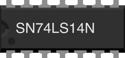
The SN74LS14N, manufactured by Texas Instruments, is a hex inverting Schmitt trigger. This component is designed to convert slow or noisy input signals into clean, fast output signals, making it ideal for applications requiring signal conditioning and noise immunity. The Schmitt trigger functionality ensures that the output transitions occur only when the input crosses specific threshold voltages, providing hysteresis and reducing susceptibility to noise.
Explore Projects Built with SN74LS14N
 Open Project in Cirkit Designer
 Open Project in Cirkit Designer
 Open Project in Cirkit Designer
 Open Project in Cirkit Designer
Explore Projects Built with SN74LS14N
Open Project in Cirkit DesignerOpen Project in Cirkit DesignerOpen Project in Cirkit DesignerOpen Project in Cirkit DesignerCommon Applications and Use Cases
- Signal conditioning in digital circuits
- Debouncing mechanical switches
- Waveform shaping and pulse generation
- Noise filtering in communication systems
- Level shifting in mixed-signal designs
Technical Specifications
The following table outlines the key technical specifications of the SN74LS14N:
| Parameter | Value |
|---|---|
| Supply Voltage (Vcc) | 4.75V to 5.25V |
| Input Voltage Range | 0V to 7V |
| High-Level Output Voltage | 2.7V (min) at 4mA |
| Low-Level Output Voltage | 0.4V (max) at 8mA |
| Input Threshold Voltage | 0.8V (low) to 2V (high) |
| Propagation Delay | 15ns (typical) |
| Power Dissipation | 20mW (typical) |
| Operating Temperature Range | 0°C to 70°C |
| Package Type | 14-pin Dual In-line Package (DIP) |
Pin Configuration and Descriptions
The SN74LS14N has 14 pins, as described in the table below:
| Pin Number | Pin Name | Description |
|---|---|---|
| 1 | 1A | Input for the first inverter |
| 2 | 1Y | Output of the first inverter |
| 3 | 2A | Input for the second inverter |
| 4 | 2Y | Output of the second inverter |
| 5 | 3A | Input for the third inverter |
| 6 | 3Y | Output of the third inverter |
| 7 | GND | Ground (0V reference) |
| 8 | 4Y | Output of the fourth inverter |
| 9 | 4A | Input for the fourth inverter |
| 10 | 5Y | Output of the fifth inverter |
| 11 | 5A | Input for the fifth inverter |
| 12 | 6Y | Output of the sixth inverter |
| 13 | 6A | Input for the sixth inverter |
| 14 | Vcc | Positive supply voltage |
Usage Instructions
How to Use the SN74LS14N in a Circuit
- Power Supply: Connect the Vcc pin (pin 14) to a regulated 5V power supply and the GND pin (pin 7) to the ground.
- Input Signal: Apply the input signal to any of the input pins (1A, 2A, 3A, 4A, 5A, or 6A). Ensure the input voltage stays within the specified range (0V to 7V).
- Output Signal: The corresponding output pin (1Y, 2Y, 3Y, 4Y, 5Y, or 6Y) will provide the inverted and conditioned signal.
- Load Considerations: Ensure the output load does not exceed the maximum current rating (8mA for low-level output and 4mA for high-level output).
Important Considerations and Best Practices
- Decoupling Capacitor: Place a 0.1µF ceramic capacitor close to the Vcc pin to filter out power supply noise.
- Unused Inputs: Tie unused input pins to Vcc or GND to prevent floating inputs, which can cause erratic behavior.
- Input Signal: Ensure the input signal transitions through the hysteresis range (0.8V to 2V) to achieve proper operation.
- Temperature Range: Operate the component within the specified temperature range (0°C to 70°C) to avoid performance degradation.
Example: Using SN74LS14N with Arduino UNO
The SN74LS14N can be used to debounce a mechanical switch and provide a clean digital signal to an Arduino UNO. Below is an example circuit and code:
Circuit Connections
- Connect the switch between the input pin (e.g., 1A) and GND.
- Use a pull-up resistor (e.g., 10kΩ) between the input pin and Vcc.
- Connect the output pin (e.g., 1Y) to an Arduino digital input pin (e.g., D2).
- Power the SN74LS14N with 5V from the Arduino's 5V pin and connect GND to the Arduino's GND.
Arduino Code
// Example code for reading a debounced switch signal using SN74LS14N
const int inputPin = 2; // Arduino pin connected to SN74LS14N output

void setup() {
  pinMode(inputPin, INPUT); // Set the pin as input
  Serial.begin(9600);       // Initialize serial communication
}

void loop() {
  int switchState = digitalRead(inputPin); // Read the switch state
  if (switchState == HIGH) {
    Serial.println("Switch is ON"); // Print message if switch is pressed
  } else {
    Serial.println("Switch is OFF"); // Print message if switch is not pressed
  }
  delay(100); // Small delay for stability
}
Troubleshooting and FAQs
Common Issues and Solutions
No Output Signal:
- Verify that the Vcc and GND pins are properly connected.
- Ensure the input signal transitions through the hysteresis range (0.8V to 2V).
- Check for loose or incorrect wiring.
Erratic Output Behavior:
- Add a decoupling capacitor (0.1µF) near the Vcc pin to reduce power supply noise.
- Tie unused input pins to Vcc or GND to prevent floating inputs.
Output Signal Not Inverted:
- Confirm that the correct input and output pins are connected.
- Verify the input signal polarity and ensure it is within the specified voltage range.
FAQs
Q: Can the SN74LS14N operate at 3.3V?
A: No, the SN74LS14N is designed to operate with a supply voltage of 4.75V to 5.25V. For 3.3V operation, consider using a different Schmitt trigger IC.
Q: What is the purpose of hysteresis in the SN74LS14N?
A: Hysteresis improves noise immunity by requiring the input signal to cross two distinct voltage thresholds (0.8V for low and 2V for high) before the output state changes. This prevents false triggering due to noise or slow signal transitions.
Q: Can I use the SN74LS14N for analog signals?
A: The SN74LS14N is designed for digital applications. While it can process slow or noisy signals, the output will always be a clean digital signal (logic high or low).