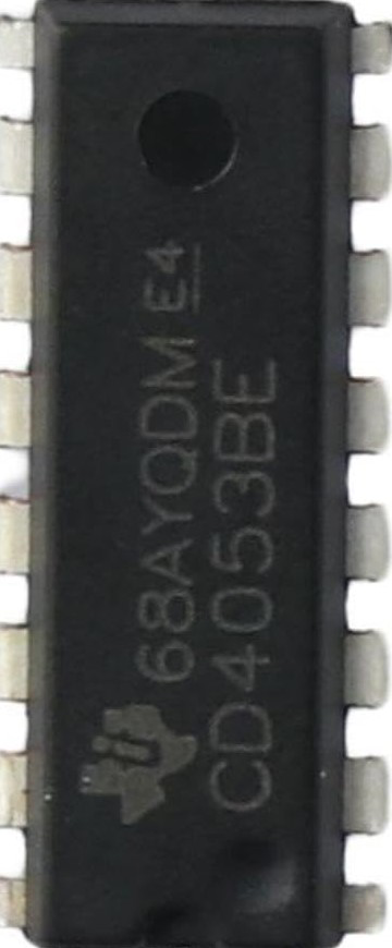
How to Use CD4053BE: Examples, Pinouts, and Specs
Introduction
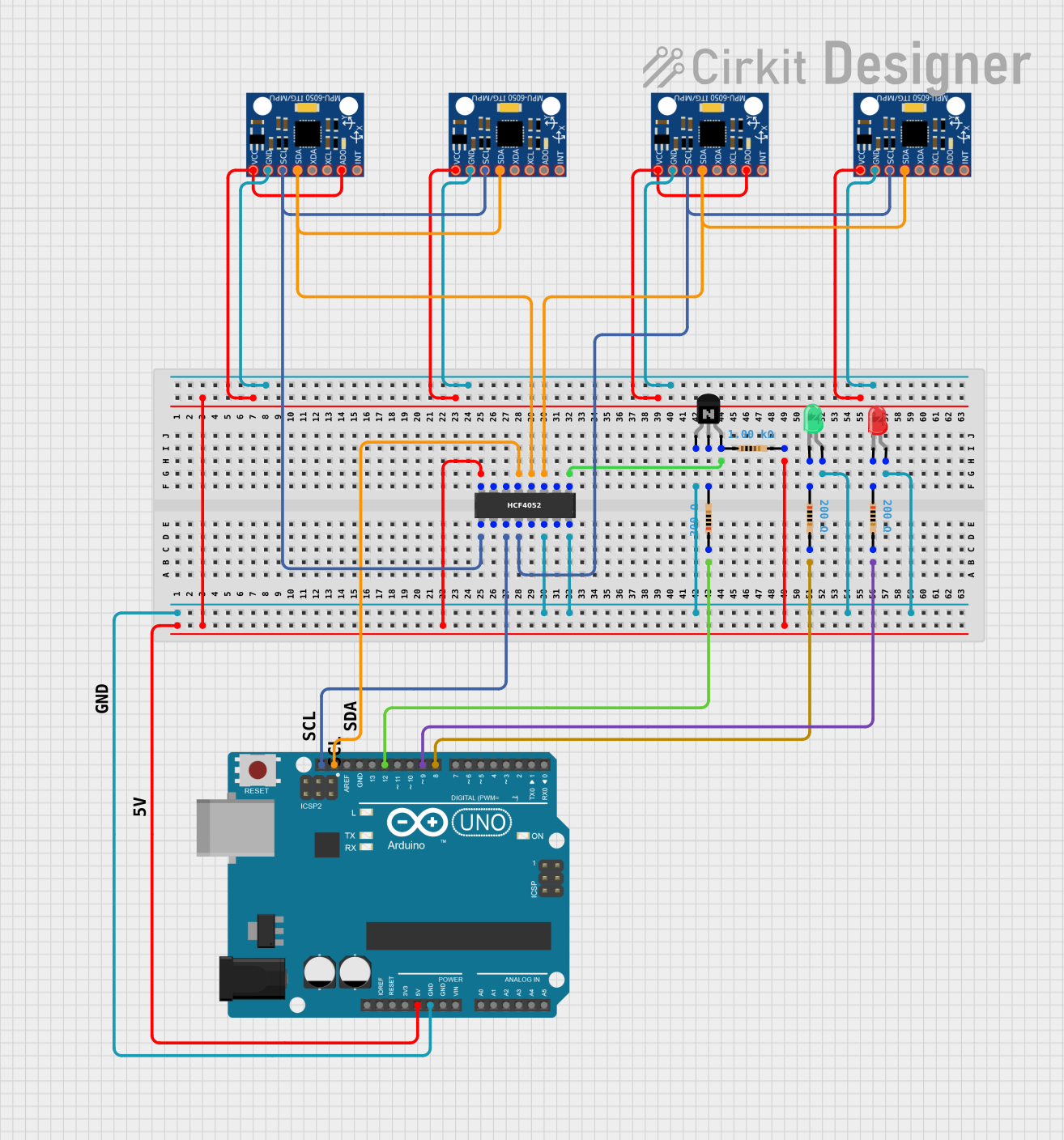
The CD4053BE is a triple 2-channel analog multiplexer/demultiplexer. It allows the selection of one of several input signals and routes it to a single output, or vice versa. This component is highly versatile and is commonly used for signal routing, analog switching, and digital logic applications. Its ability to handle both analog and digital signals makes it suitable for a wide range of applications, including audio signal processing, data acquisition systems, and microcontroller-based projects.
Explore Projects Built with CD4053BE
Explore Projects Built with CD4053BE
Technical Specifications
- Type: Triple 2-channel analog multiplexer/demultiplexer
- Operating Voltage Range: 3V to 20V
- Maximum Input Current: ±10mA
- On-State Resistance (RON): 125Ω (typical) at VDD = 10V
- Switching Speed: 125ns (typical) at VDD = 10V
- Operating Temperature Range: -55°C to +125°C
- Package Type: PDIP-16 (Plastic Dual In-line Package)
Pin Configuration and Descriptions
The CD4053BE has 16 pins, as described in the table below:
| Pin Number | Pin Name | Description |
|---|---|---|
| 1 | INH | Inhibit input (active HIGH, disables all switches when HIGH) |
| 2 | A | Control input for Channel A |
| 3 | B | Control input for Channel B |
| 4 | C | Control input for Channel C |
| 5 | A1 | Channel A input/output 1 |
| 6 | A0 | Channel A input/output 0 |
| 7 | B1 | Channel B input/output 1 |
| 8 | VSS | Negative supply voltage (commonly connected to GND) |
| 9 | B0 | Channel B input/output 0 |
| 10 | C1 | Channel C input/output 1 |
| 11 | C0 | Channel C input/output 0 |
| 12 | VEE | Negative voltage for analog signals (commonly connected to GND for single-supply) |
| 13 | VDD | Positive supply voltage |
| 14 | A2 | Common terminal for Channel A |
| 15 | B2 | Common terminal for Channel B |
| 16 | C2 | Common terminal for Channel C |
Usage Instructions
How to Use the CD4053BE in a Circuit
- Power Supply: Connect the VDD pin to the positive supply voltage (e.g., 5V or 12V) and the VSS pin to ground. If using a single-supply configuration, connect VEE to ground as well.
- Control Inputs: Use the A, B, and C control pins to select the desired input/output channel for each multiplexer. A logic LOW (0) or HIGH (1) on these pins determines which channel is active.
- Signal Routing: Connect the input/output signals to the A0/A1, B0/B1, and C0/C1 pins. The selected signal will be routed to the corresponding common terminal (A2, B2, or C2).
- Inhibit Function: If the INH pin is set HIGH, all switches will be disabled, regardless of the control inputs.
Important Considerations and Best Practices
- Ensure that the input signal voltage does not exceed the supply voltage range (VSS to VDD).
- For optimal performance, minimize the load capacitance on the signal lines to reduce switching delays.
- Use decoupling capacitors (e.g., 0.1µF) near the VDD pin to stabilize the power supply.
- If using the CD4053BE with an Arduino or other microcontroller, ensure that the control signals are within the logic level range of the IC.
Example: Connecting the CD4053BE to an Arduino UNO
Below is an example of how to control the CD4053BE using an Arduino UNO to switch between two analog signals:
// Define control pins for the CD4053BE
const int controlPinA = 2; // Control pin for Channel A
const int controlPinB = 3; // Control pin for Channel B
const int controlPinC = 4; // Control pin for Channel C

void setup() {
  // Set control pins as outputs
  pinMode(controlPinA, OUTPUT);
  pinMode(controlPinB, OUTPUT);
  pinMode(controlPinC, OUTPUT);
}

void loop() {
  // Example: Switch Channel A to A0
  digitalWrite(controlPinA, LOW); // Set A control pin to LOW
  delay(1000); // Wait for 1 second

  // Example: Switch Channel A to A1
  digitalWrite(controlPinA, HIGH); // Set A control pin to HIGH
  delay(1000); // Wait for 1 second
}
In this example, the Arduino controls the A channel of the CD4053BE, toggling between the A0 and A1 inputs every second. Similar logic can be applied to control the B and C channels.
Troubleshooting and FAQs
Common Issues
No Signal Output:
- Ensure that the INH pin is set to LOW. If it is HIGH, all switches will be disabled.
- Verify that the control pins (A, B, C) are receiving the correct logic levels.
Signal Distortion:
- Check that the input signal voltage is within the supply voltage range.
- Minimize the load capacitance and ensure proper grounding to reduce noise.
Switching Delays:
- Ensure that the control signals are stable and not fluctuating.
- Use a higher supply voltage (within the IC's limits) to reduce on-state resistance and improve switching speed.
FAQs
Q: Can the CD4053BE handle digital signals?
A: Yes, the CD4053BE can handle both analog and digital signals, provided the signal voltage is within the supply voltage range.
Q: What is the purpose of the VEE pin?
A: The VEE pin is used for negative voltage in dual-supply configurations. For single-supply operation, it should be connected to ground.
Q: How do I prevent crosstalk between channels?
A: To minimize crosstalk, use proper PCB layout techniques, such as keeping signal traces short and separating high-frequency signals from sensitive analog lines.
This concludes the documentation for the CD4053BE.