
How to Use 4049: Examples, Pinouts, and Specs

 Design with 4049 in Cirkit Designer
Introduction
The 4049 integrated circuit (IC) is a versatile component that features six independent inverter gates. These gates are capable of converting digital signals from one logic level to another, making it an essential tool for interfacing electronics that operate at different voltage levels. The 4049 is commonly used for level shifting, logic inversion, and signal buffering in a variety of applications, including digital electronics, signal processing, and microcontroller interfacing.
Explore Projects Built with 4049
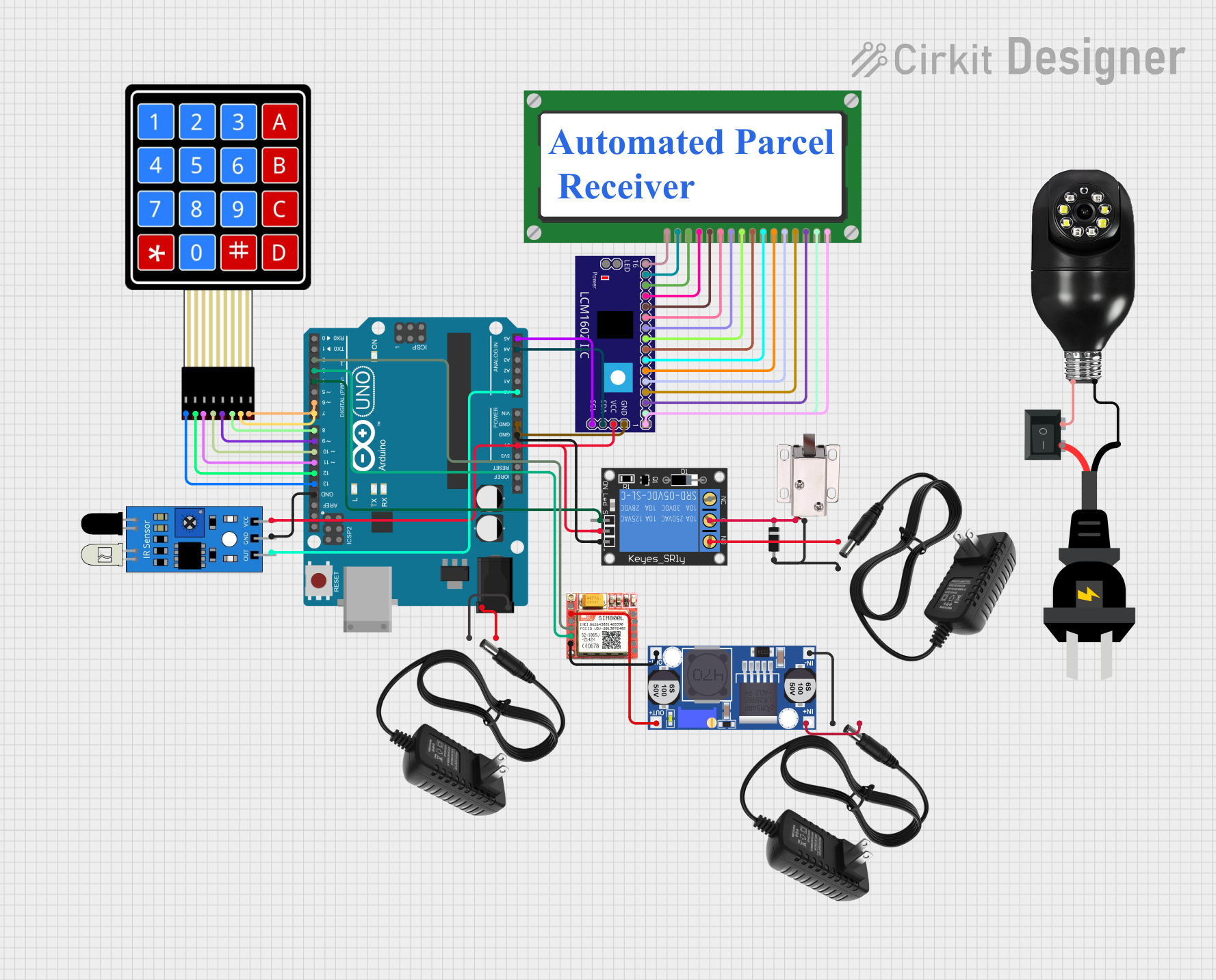
 Open Project in Cirkit Designer
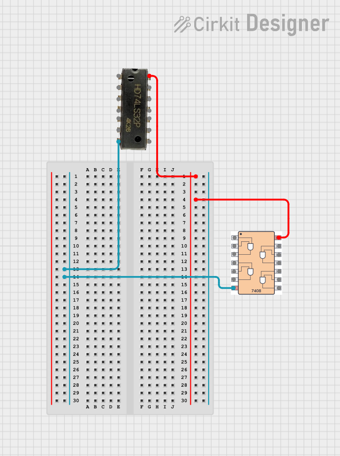
 Open Project in Cirkit Designer
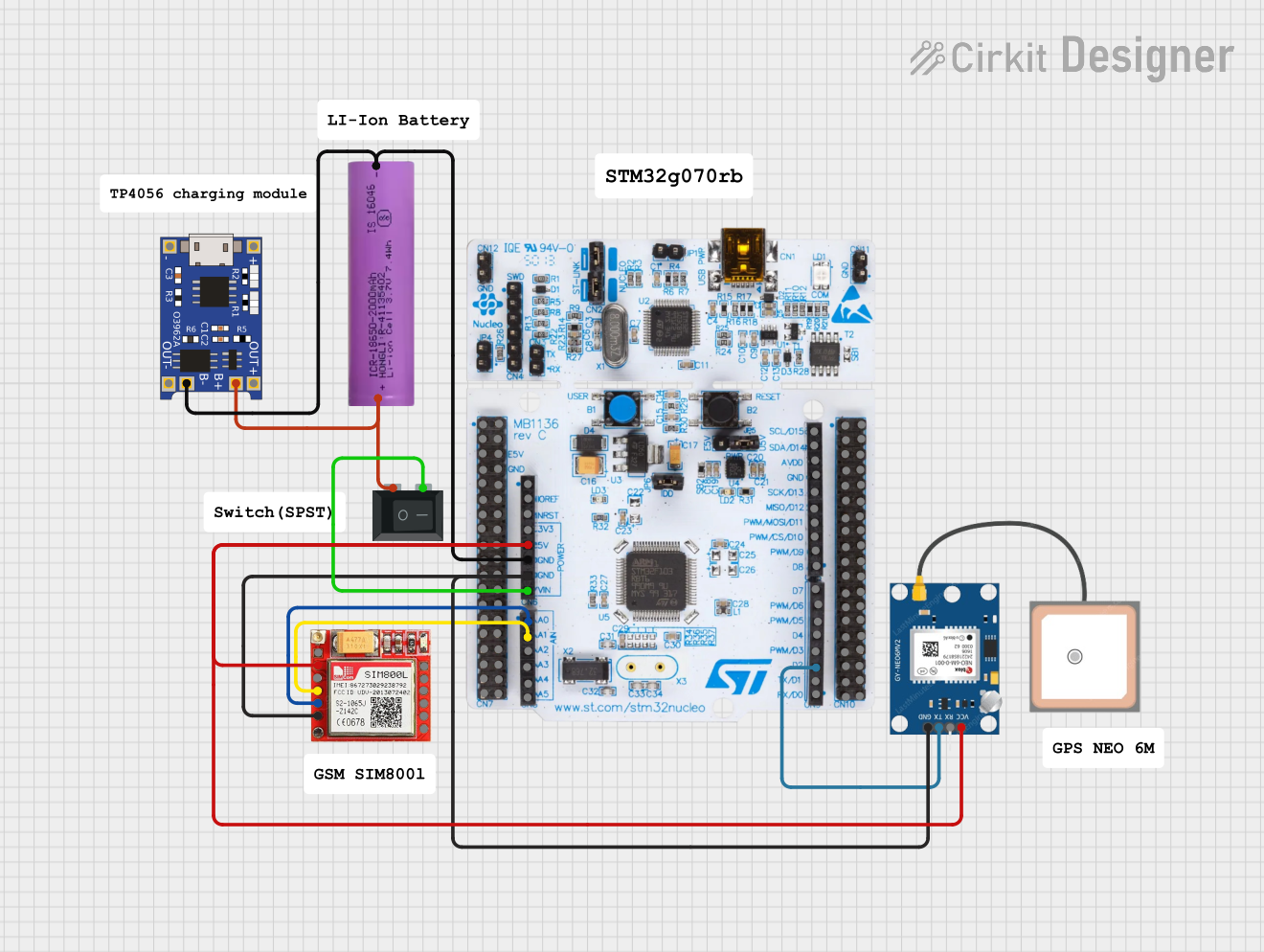
 Open Project in Cirkit Designer
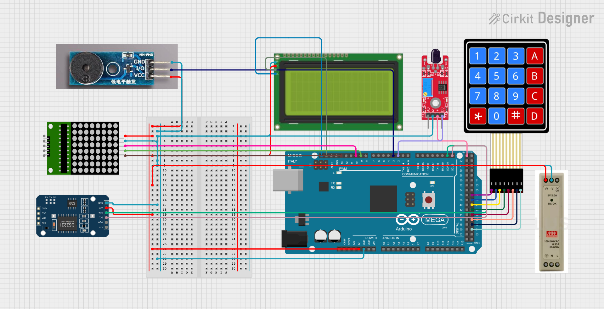
 Open Project in Cirkit Designer
Explore Projects Built with 4049

 Open Project in Cirkit Designer
 Open Project in Cirkit Designer
 Open Project in Cirkit Designer
 Open Project in Cirkit Designer
Common Applications
- Logic level conversion
- Signal buffering and amplification
- Oscillator circuits
- Waveform shaping
- Glitch elimination in digital signals
Technical Specifications
Key Technical Details
- Supply Voltage (VCC): 3V to 18V
- High-Level Input Voltage (VIH): 3.5V min (VCC = 15V)
- Low-Level Input Voltage (VIL): 1.5V max (VCC = 15V)
- High-Level Output Current (IOH): -0.4mA max (VCC = 15V)
- Low-Level Output Current (IOL): 4.8mA max (VCC = 15V)
- Propagation Delay Time: 30ns typ (VCC = 10V, CL = 50pF)
Pin Configuration and Descriptions
| Pin Number | Name | Description |
|---|---|---|
| 1 | A1 | Input of inverter 1 |
| 2 | Y1 | Output of inverter 1 |
| 3 | A2 | Input of inverter 2 |
| 4 | Y2 | Output of inverter 2 |
| 5 | A3 | Input of inverter 3 |
| 6 | Y3 | Output of inverter 3 |
| 7 | GND | Ground (0V) |
| 8 | Y4 | Output of inverter 4 |
| 9 | A4 | Input of inverter 4 |
| 10 | Y5 | Output of inverter 5 |
| 11 | A5 | Input of inverter 5 |
| 12 | Y6 | Output of inverter 6 |
| 13 | A6 | Input of inverter 6 |
| 14 | VCC | Positive Supply Voltage |
Usage Instructions
How to Use the 4049 in a Circuit
Power Supply Connection: Connect pin 14 (VCC) to the positive supply voltage within the specified range (3V to 18V). Connect pin 7 (GND) to the ground of the circuit.
Input Connection: Apply the input signal to the input pin (A1 to A6) of the desired inverter gate.
Output Connection: The output signal can be taken from the corresponding output pin (Y1 to Y6).
Bypass Capacitor: It is recommended to use a 0.1µF bypass capacitor between VCC and GND near the IC to filter out noise.
Important Considerations and Best Practices
- Ensure that the supply voltage does not exceed the maximum rating to prevent damage.
- Unused inputs should be tied to VCC or GND to avoid floating inputs which can lead to erratic behavior.
- When using the IC for level shifting, make sure the input signal's voltage levels are compatible with the IC's specified input voltage range.
- The output current should not exceed the specified limits to maintain signal integrity and prevent overheating.
Troubleshooting and FAQs
Common Issues
- Signal Distortion: Ensure that the supply voltage is stable and within the recommended range. Check for proper decoupling with a bypass capacitor.
- Unexpected Output: Verify that all unused inputs are tied to a defined logic level. Floating inputs can cause unpredictable behavior.
- Overheating: Confirm that the output current does not exceed the maximum ratings. Excessive current draw can lead to increased temperature and potential failure.
FAQs
Q: Can the 4049 be used with a 5V logic system? A: Yes, the 4049 can be used with a 5V logic system, as its operating voltage range starts from 3V.
Q: Is it necessary to use all six inverters? A: No, it is not necessary to use all six inverters. However, ensure that the inputs of unused inverters are tied to a known logic level.
Q: Can the 4049 be used to drive LEDs or other indicators? A: Yes, the 4049 can drive LEDs or other indicators, provided the current requirements do not exceed the output current specifications.
Example Code for Arduino UNO
The following example demonstrates how to use the 4049 IC with an Arduino UNO for simple logic inversion.
// Define the input and output pins
const int inputPin = 2;  // Connect to A1 of 4049
const int outputPin = 3; // Connect to Y1 of 4049

void setup() {
  pinMode(inputPin, INPUT);
  pinMode(outputPin, OUTPUT);
}

void loop() {
  // Read the state of the input pin
  int inputState = digitalRead(inputPin);

  // Invert the state and output to the output pin
  digitalWrite(outputPin, !inputState);
}
Remember to connect the Arduino's GND to pin 7 (GND) of the 4049 and VCC to pin 14 (VCC) with the appropriate supply voltage for the IC. The input signal from the Arduino is connected to pin 1 (A1), and the inverted output can be taken from pin 2 (Y1).