How to Use SN74AHCT125N : Examples, Pinouts, and Specs
Introduction
The SN74AHCT125N is a quad bus buffer gate with 3-state outputs from Texas Instruments. This integrated circuit is designed to provide high-speed, TTL-compatible operation, making it suitable for interfacing with TTL logic levels while driving loads with a higher current capability. The 3-state outputs allow for connection to a bus-oriented system, where multiple outputs can share a common connection without interference.
Common applications for the SN74AHCT125N include:
- Driving bus lines or buffer memory address registers
- Data transmission systems with multiple data sources
- Digital signal isolation and level shifting
- Interfacing between different logic families
Explore Projects Built with SN74AHCT125N
Explore Projects Built with SN74AHCT125N
Technical Specifications
Key Technical Details
- Supply Voltage (Vcc): 4.5V to 5.5V
- High-Level Output Current (IOH): -8 mA
- Low-Level Output Current (IOL): 8 mA
- Input Capacitance (Ci): 3 pF (typical)
- Propagation Delay (tpd): 11 ns (max)
- Operating Temperature Range: -40°C to 85°C
Pin Configuration and Descriptions
| Pin Number | Name | Description |
|---|---|---|
| 1 | 1OE | Output enable for buffer 1 (active low) |
| 2 | 1A | Input for buffer 1 |
| 3 | 1Y | Output for buffer 1 |
| 4 | 2OE | Output enable for buffer 2 (active low) |
| 5 | 2A | Input for buffer 2 |
| 6 | 2Y | Output for buffer 2 |
| 7 | GND | Ground (0V) |
| 8 | 3Y | Output for buffer 3 |
| 9 | 3A | Input for buffer 3 |
| 10 | 3OE | Output enable for buffer 3 (active low) |
| 11 | 4Y | Output for buffer 4 |
| 12 | 4A | Input for buffer 4 |
| 13 | 4OE | Output enable for buffer 4 (active low) |
| 14 | Vcc | Positive supply voltage |
Usage Instructions
How to Use the SN74AHCT125N in a Circuit
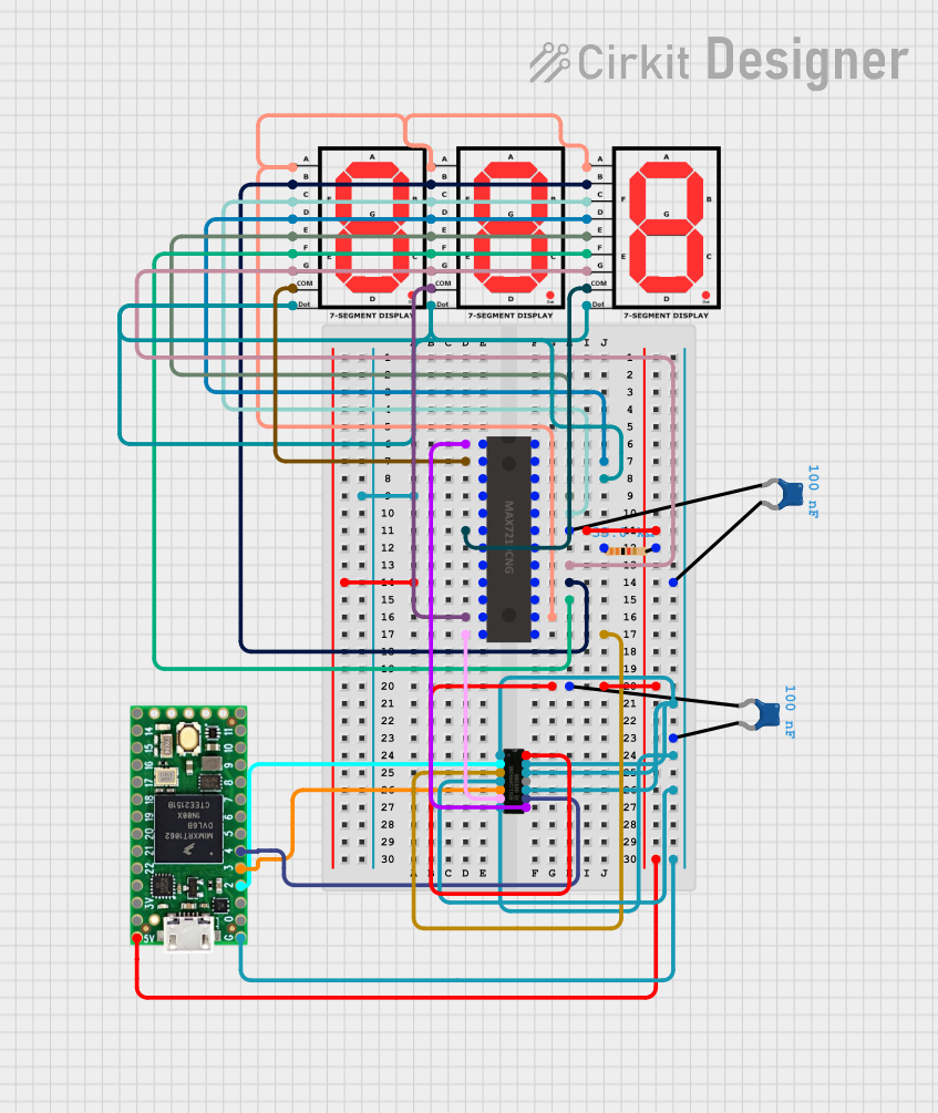
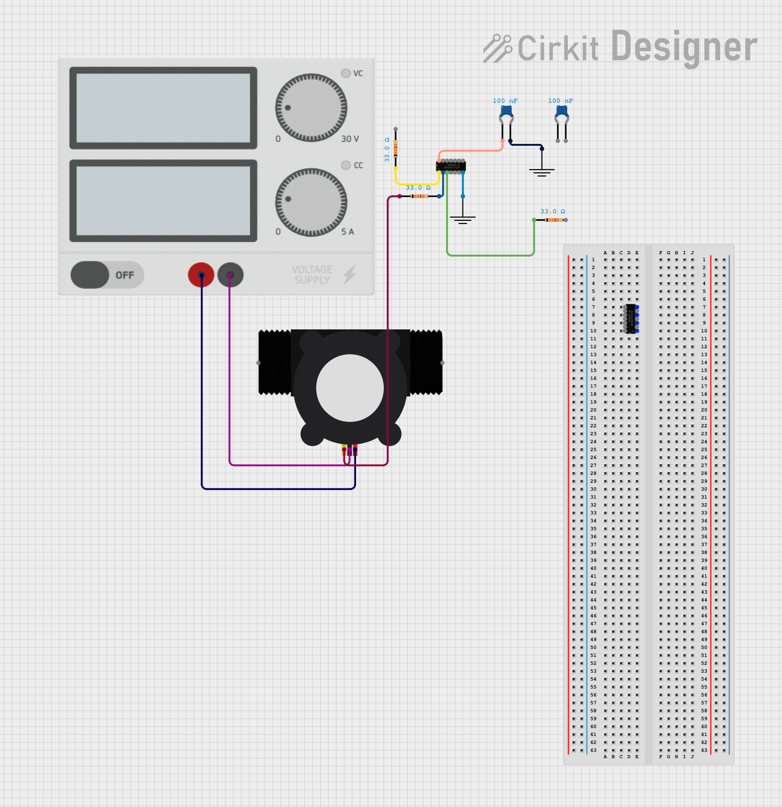
Power Supply Connection: Connect Vcc (pin 14) to a 5V power supply and GND (pin 7) to the ground of your circuit.
Input Connection: Apply the input signal to the input pins (1A, 2A, 3A, 4A) as required for your application.
Output Enable: To activate the output of each buffer, connect the respective output enable pin (1OE, 2OE, 3OE, 4OE) to a low logic level (GND). To disable the output (high impedance state), connect the output enable pin to a high logic level (Vcc).
Output Connection: Connect the output pins (1Y, 2Y, 3Y, 4Y) to the next stage in your circuit. Ensure that the load connected does not exceed the specified output current limits.
Important Considerations and Best Practices
Decoupling Capacitors: Place a 0.1 µF ceramic decoupling capacitor close to the Vcc pin to filter out noise and stabilize the power supply.
Output Load: Do not exceed the maximum specified output current to prevent damage to the device.
Unused Inputs: Connect unused input pins to a defined logic level (either Vcc or GND) to prevent floating inputs which can lead to increased power consumption and erratic behavior.
Temperature Range: Ensure that the operating temperature remains within the specified range for reliable performance.
Troubleshooting and FAQs
Common Issues
Outputs Not Switching: Ensure that the output enable pins are correctly driven to a low logic level to enable the outputs.
Unexpected Logic Levels: Check that all inputs are connected to a valid logic level and are not floating.
Device Heating Up: Verify that the power supply voltage is within the specified range and that the output current is not exceeding the maximum limits.
Solutions and Tips for Troubleshooting
Check Connections: Double-check all connections, especially the power supply and ground connections.
Measure Voltages: Use a multimeter to measure the supply voltage at the Vcc pin and the logic levels at the input and output enable pins.
Isolate the Problem: If the circuit is complex, isolate the SN74AHCT125N and test it in a simpler configuration to ensure it is functioning correctly.
FAQs
Q: Can I use the SN74AHCT125N at voltages lower than 4.5V? A: The SN74AHCT125N is designed to operate within a supply voltage range of 4.5V to 5.5V. Operating it outside this range may result in improper functioning or damage to the device.
Q: How do I put the outputs in a high impedance state? A: To place the outputs in a high impedance state, drive the respective output enable pin (OE) to a high logic level (Vcc).
Q: Can I use this buffer to interface 3.3V logic with 5V logic? A: Yes, the SN74AHCT125N can be used for level shifting. Ensure that the input logic levels are compatible with TTL levels and that the Vcc is connected to the higher voltage level.
Example Code for Arduino UNO
// Example code to drive an SN74AHCT125N buffer with an Arduino UNO

const int enablePin = 2; // Connect to 1OE on the SN74AHCT125N
const int inputPin = 3;  // Connect to 1A on the SN74AHCT125N
const int outputPin = 4; // Connect to 1Y on the SN74AHCT125N (Monitor this pin)

void setup() {
  pinMode(enablePin, OUTPUT);
  pinMode(inputPin, OUTPUT);
  pinMode(outputPin, INPUT); // Set as input for monitoring purposes

  // Enable the buffer output
  digitalWrite(enablePin, LOW);
}

void loop() {
  // Send a high signal through the buffer
  digitalWrite(inputPin, HIGH);
  delay(1000); // Wait for 1 second

  // Send a low signal through the buffer
  digitalWrite(inputPin, LOW);
  delay(1000); // Wait for 1 second
}
This example demonstrates how to control the SN74AHCT125N using an Arduino UNO. The code toggles the input to the buffer and enables the output, allowing you to monitor the output state with an external device or oscilloscope. Remember to adjust the pin numbers as per your actual connection setup.