
How to Use AD9835: Examples, Pinouts, and Specs
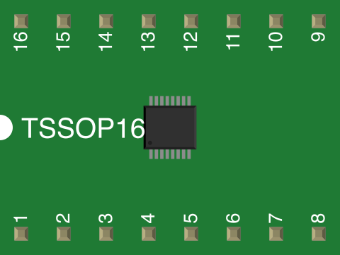
 Design with AD9835 in Cirkit Designer
Introduction
The AD9835 is a low-power, programmable waveform generator manufactured by Analog Devices. It is capable of producing sine, triangle, and square waveforms with a frequency resolution of up to 28 bits. The device is controlled via a serial interface, making it highly versatile and suitable for a wide range of applications.
Explore Projects Built with AD9835
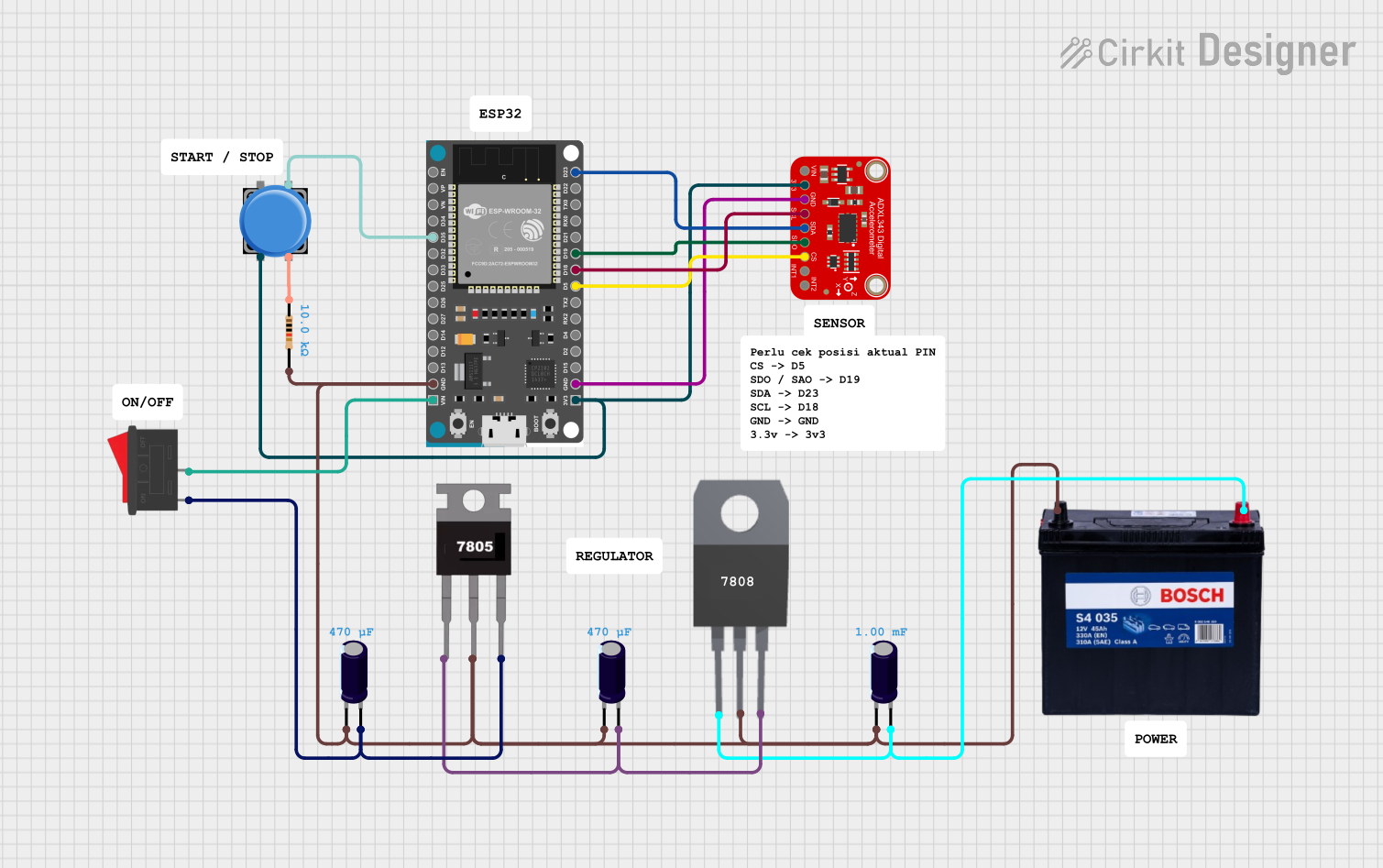 Open Project in Cirkit Designer
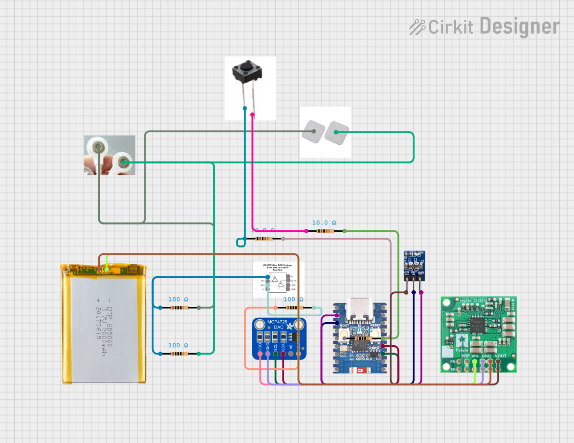 Open Project in Cirkit Designer
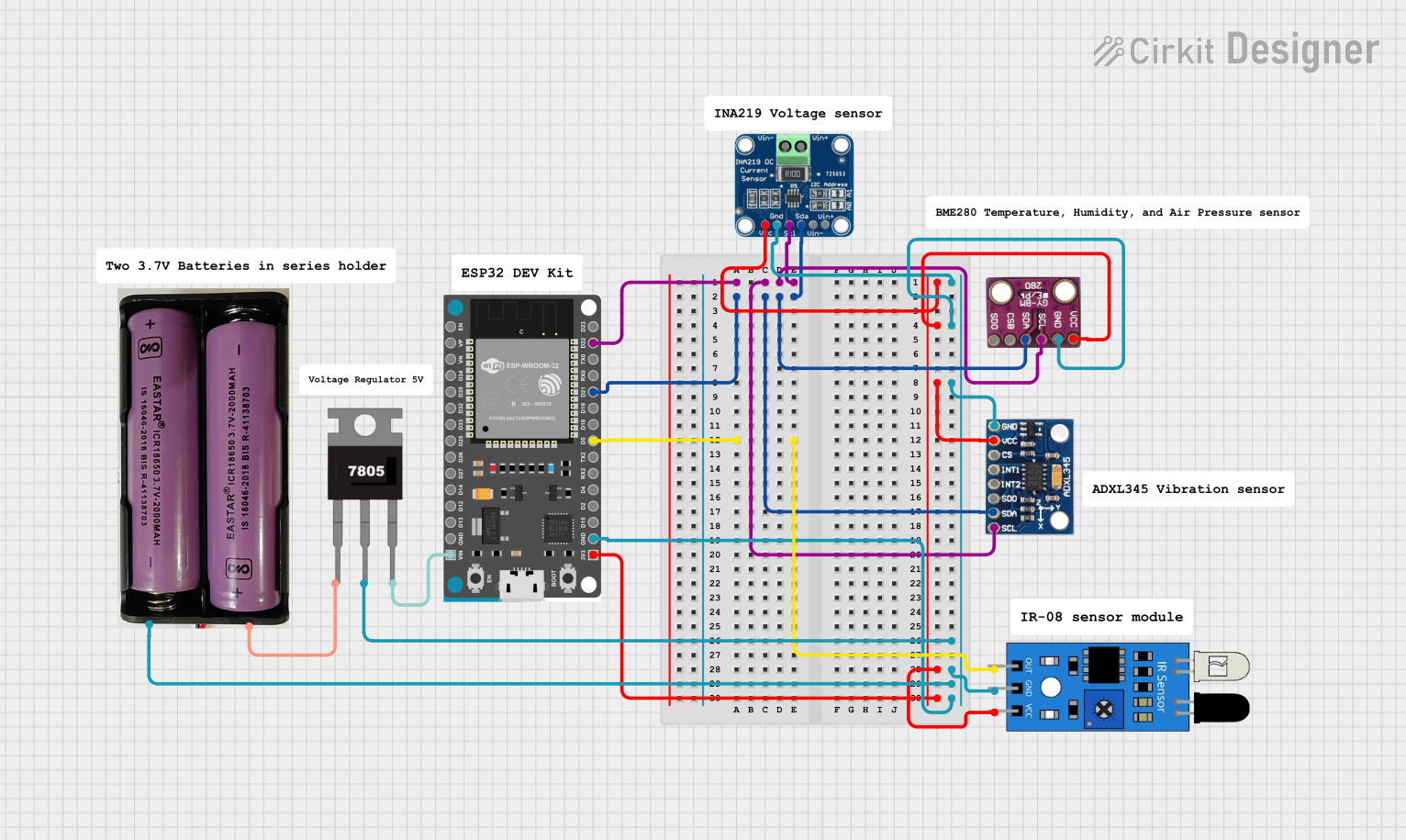 Open Project in Cirkit Designer
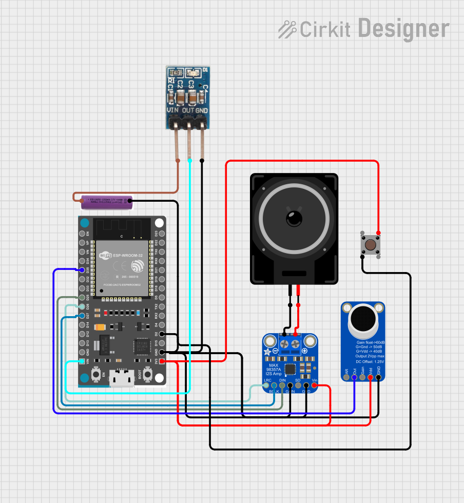 Open Project in Cirkit Designer
Explore Projects Built with AD9835
Open Project in Cirkit DesignerOpen Project in Cirkit DesignerOpen Project in Cirkit DesignerOpen Project in Cirkit DesignerCommon Applications
- Signal generation for testing and measurement equipment
- Frequency modulation (FM) and phase modulation (PM) systems
- Function generators
- Audio signal synthesis
- Communications systems
Technical Specifications
Below are the key technical details of the AD9835:
| Parameter | Value |
|---|---|
| Supply Voltage (VDD) | 2.3 V to 5.5 V |
| Power Consumption | 20 mW (typical at 3 V) |
| Frequency Resolution | 28 bits |
| Maximum Output Frequency | 25 MHz |
| Output Waveforms | Sine, Triangle, Square |
| Serial Interface | SPI-compatible, 3-wire |
| Operating Temperature Range | -40°C to +85°C |
| Package Type | TSSOP-20 (AD9835BRUZ) |
Pin Configuration and Descriptions
The AD9835 comes in a 20-pin TSSOP package. Below is the pin configuration and description:
| Pin Number | Pin Name | Description |
|---|---|---|
| 1 | VDD | Positive power supply (2.3 V to 5.5 V). |
| 2 | DGND | Digital ground. |
| 3 | MCLK | Master clock input. Determines the frequency of the output waveform. |
| 4 | FSELECT | Frequency select pin. Chooses between two frequency registers. |
| 5 | PSELECT | Phase select pin. Chooses between two phase registers. |
| 6 | RESET | Active high reset pin. Resets internal registers. |
| 7 | SCLK | Serial clock input for SPI communication. |
| 8 | SDATA | Serial data input for SPI communication. |
| 9 | FSYNC | Frame synchronization signal for SPI communication. |
| 10 | AGND | Analog ground. |
| 11 | IOUT | Current output. Connect to a load resistor to generate voltage output. |
| 12 | COMP | Compensation pin. Connect to a capacitor for stability. |
| 13-20 | NC | No connection. Leave these pins unconnected. |
Usage Instructions
How to Use the AD9835 in a Circuit
- Power Supply: Connect the VDD pin to a stable power supply (2.3 V to 5.5 V) and connect DGND and AGND to ground.
- Clock Input: Provide a stable clock signal to the MCLK pin. The clock frequency determines the maximum output frequency.
- SPI Communication:
- Use the SCLK, SDATA, and FSYNC pins to configure the device via an SPI-compatible interface.
- Write to the frequency and phase registers to set the desired waveform parameters.
- Output: Connect a load resistor to the IOUT pin to generate a voltage output. Optionally, use a low-pass filter to smooth the output waveform.
Important Considerations
- Clock Stability: Ensure the master clock (MCLK) is stable to avoid jitter in the output waveform.
- Output Filtering: Use an external low-pass filter to remove high-frequency components from the output signal.
- Reset: Use the RESET pin to initialize the device before programming it.
- SPI Timing: Follow the SPI timing requirements specified in the datasheet to ensure reliable communication.
Example: Interfacing AD9835 with Arduino UNO
Below is an example of how to interface the AD9835 with an Arduino UNO to generate a sine wave:
#include <SPI.h>

// Pin definitions for AD9835
#define FSYNC 10  // Connect to FSYNC pin of AD9835
#define SCLK  13  // Connect to SCLK pin of AD9835
#define SDATA 11  // Connect to SDATA pin of AD9835

void setup() {
  // Initialize SPI
  SPI.begin();
  pinMode(FSYNC, OUTPUT);
  digitalWrite(FSYNC, HIGH); // Set FSYNC high initially

  // Reset AD9835
  writeRegister(0x2100); // Reset command
  delay(10);

  // Set frequency to 1 kHz (example value)
  setFrequency(1000);

  // Exit reset mode
  writeRegister(0x2000); // Clear reset bit
}

void loop() {
  // The waveform will continue to generate without further code
}

// Function to write a 16-bit value to the AD9835
void writeRegister(uint16_t data) {
  digitalWrite(FSYNC, LOW); // Enable communication
  SPI.transfer(highByte(data)); // Send high byte
  SPI.transfer(lowByte(data));  // Send low byte
  digitalWrite(FSYNC, HIGH); // Disable communication
}

// Function to set frequency (example: 1 kHz)
void setFrequency(uint32_t frequency) {
  uint32_t freqWord = (frequency * 268435456UL) / 25000000UL; // Calculate frequency word
  writeRegister(0x4000 | (freqWord & 0x3FFF)); // Write lower 14 bits
  writeRegister(0x4000 | ((freqWord >> 14) & 0x3FFF)); // Write upper 14 bits
}
Notes:
- Replace
25000000ULwith the actual clock frequency (MCLK) in Hz. - Use appropriate resistors and capacitors for the output stage to match your application requirements.
Troubleshooting and FAQs
Common Issues
No Output Signal:
- Ensure the power supply is within the specified range (2.3 V to 5.5 V).
- Verify that the SPI communication is functioning correctly.
- Check that the RESET pin is properly initialized.
Distorted Waveform:
- Use a low-pass filter to remove high-frequency noise.
- Ensure the load resistor on the IOUT pin is correctly chosen.
Incorrect Frequency Output:
- Verify the master clock (MCLK) frequency.
- Double-check the frequency word calculation in your code.
FAQs
Q: Can the AD9835 generate arbitrary waveforms?
A: No, the AD9835 is limited to sine, triangle, and square waveforms. For arbitrary waveforms, consider using a DAC with waveform memory.
Q: What is the maximum output frequency?
A: The maximum output frequency is 25 MHz, but the actual usable frequency depends on the master clock and application requirements.
Q: How do I improve waveform accuracy?
A: Use a stable clock source, minimize noise in the power supply, and apply proper filtering to the output signal.
Q: Can I use the AD9835 with a 3.3 V microcontroller?
A: Yes, the AD9835 operates with a supply voltage as low as 2.3 V, making it compatible with 3.3 V systems. Ensure proper logic level matching for SPI communication.