How to Use 74ls173: Examples, Pinouts, and Specs
Introduction
The 74LS173 is a quad D-type flip-flop manufactured by Texas Instruments. It features four D-type flip-flops with a common clock input and active-low enable inputs. This component is widely used in digital circuits for data storage and transfer, enabling the synchronization of data with a clock signal. Its compact design and reliable performance make it a popular choice in applications requiring temporary data storage or controlled data flow.
Explore Projects Built with 74ls173

Explore Projects Built with 74ls173
Common Applications
- Data latching and storage in digital systems
- Buffering and synchronization of data
- Shift registers and counters
- Memory addressing and control logic
Technical Specifications
The following table outlines the key technical details of the 74LS173:
| Parameter | Value |
|---|---|
| Supply Voltage (Vcc) | 4.75V to 5.25V |
| Input Voltage (VI) | 0V to 7V |
| High-Level Output Voltage | 2.7V (min) |
| Low-Level Output Voltage | 0.4V (max) |
| High-Level Input Current | 20 µA (max) |
| Low-Level Input Current | -0.4 mA (max) |
| Propagation Delay (typical) | 20 ns |
| Operating Temperature Range | 0°C to 70°C |
| Package Type | DIP-16, SOIC-16 |
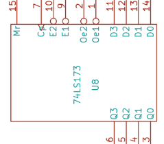
Pin Configuration and Descriptions
The 74LS173 comes in a 16-pin package. The pinout and descriptions are as follows:
| Pin Number | Pin Name | Description |
|---|---|---|
| 1 | MR | Master Reset (Active Low) |
| 2 | G1 | Enable Input 1 (Active Low) |
| 3 | G2 | Enable Input 2 (Active Low) |
| 4 | D0 | Data Input 0 |
| 5 | D1 | Data Input 1 |
| 6 | D2 | Data Input 2 |
| 7 | D3 | Data Input 3 |
| 8 | GND | Ground |
| 9 | Q3 | Data Output 3 |
| 10 | Q2 | Data Output 2 |
| 11 | Q1 | Data Output 1 |
| 12 | Q0 | Data Output 0 |
| 13 | CLK | Clock Input |
| 14 | OE1 | Output Enable 1 (Active Low) |
| 15 | OE2 | Output Enable 2 (Active Low) |
| 16 | Vcc | Positive Supply Voltage |
Usage Instructions
The 74LS173 is straightforward to use in digital circuits. Below are the steps and considerations for proper usage:
Basic Circuit Connection
- Power Supply: Connect pin 16 (Vcc) to a 5V power supply and pin 8 (GND) to ground.
- Clock Signal: Provide a clock signal to pin 13 (CLK) to synchronize data storage and transfer.
- Data Inputs: Connect the data inputs (D0–D3) to the desired data source.
- Enable Inputs: Ensure that both enable inputs (G1 and G2) are held low to enable the flip-flops.
- Output Enable: To activate the outputs (Q0–Q3), set both OE1 and OE2 to low. If either is high, the outputs will be in a high-impedance state.
- Master Reset: Use the MR pin to reset all outputs to low. This pin is active low, so it must be held high during normal operation.
Example Circuit with Arduino UNO
The 74LS173 can be interfaced with an Arduino UNO for data storage and control. Below is an example code snippet:
// Example: Interfacing 74LS173 with Arduino UNO
// This code demonstrates how to control the 74LS173 flip-flop using Arduino.

// Pin definitions
const int clkPin = 2;  // Clock signal
const int mrPin = 3;   // Master Reset
const int g1Pin = 4;   // Enable Input 1
const int g2Pin = 5;   // Enable Input 2
const int dPins[] = {6, 7, 8, 9}; // Data inputs D0-D3

void setup() {
  // Set pin modes
  pinMode(clkPin, OUTPUT);
  pinMode(mrPin, OUTPUT);
  pinMode(g1Pin, OUTPUT);
  pinMode(g2Pin, OUTPUT);
  for (int i = 0; i < 4; i++) {
    pinMode(dPins[i], OUTPUT);
  }

  // Initialize pins
  digitalWrite(mrPin, HIGH);  // Disable reset
  digitalWrite(g1Pin, LOW);   // Enable flip-flops
  digitalWrite(g2Pin, LOW);   // Enable flip-flops
  digitalWrite(clkPin, LOW);  // Initialize clock
}

void loop() {
  // Example: Store and transfer data
  for (int i = 0; i < 16; i++) {
    // Set data inputs
    for (int j = 0; j < 4; j++) {
      digitalWrite(dPins[j], (i >> j) & 0x01); // Set each bit of D0-D3
    }

    // Generate clock pulse
    digitalWrite(clkPin, HIGH);
    delay(10); // Short delay for clock pulse
    digitalWrite(clkPin, LOW);
    delay(10);
  }
}
Best Practices
- Use decoupling capacitors (e.g., 0.1 µF) near the Vcc pin to reduce noise and ensure stable operation.
- Avoid floating inputs by connecting unused inputs to a defined logic level (e.g., GND or Vcc).
- Ensure the clock signal is clean and free of noise to prevent unintended behavior.
Troubleshooting and FAQs
Common Issues
Outputs Not Responding:
- Check if the enable inputs (G1 and G2) are both low.
- Verify that the output enable pins (OE1 and OE2) are low.
- Ensure the clock signal is properly connected and functioning.
Unexpected Output States:
- Confirm that the data inputs (D0–D3) are correctly set before the clock pulse.
- Check for noise or glitches on the clock line.
Outputs Stuck in High-Impedance:
- Verify that both OE1 and OE2 are low. If either is high, the outputs will be disabled.
FAQs
Q1: Can the 74LS173 operate at 3.3V?
No, the 74LS173 is designed to operate within a supply voltage range of 4.75V to 5.25V. Using it at 3.3V may result in unreliable operation.
Q2: What happens if the MR pin is left floating?
The MR pin is active low and should not be left floating. If left unconnected, it may cause unpredictable behavior. Connect it to Vcc for normal operation or to GND to reset the outputs.
Q3: How do I cascade multiple 74LS173 ICs?
To cascade multiple ICs, connect the clock and enable inputs in parallel. Use the outputs of one IC as the inputs to the next stage for extended data storage or transfer.
By following this documentation, users can effectively integrate the 74LS173 into their digital circuits for reliable data storage and synchronization.