
How to Use AD7302: Examples, Pinouts, and Specs
 Design with AD7302 in Cirkit Designer
Introduction
The AD7302 is a dual 12-bit digital-to-analog converter (DAC) manufactured by Analog Devices. It is designed to deliver high performance with low power consumption, making it ideal for a wide range of applications. The AD7302 features a serial interface, which simplifies integration into digital systems. Its compact design and robust functionality make it suitable for use in audio systems, instrumentation, control systems, and other precision applications.
Explore Projects Built with AD7302
 Open Project in Cirkit Designer
 Open Project in Cirkit Designer
 Open Project in Cirkit Designer
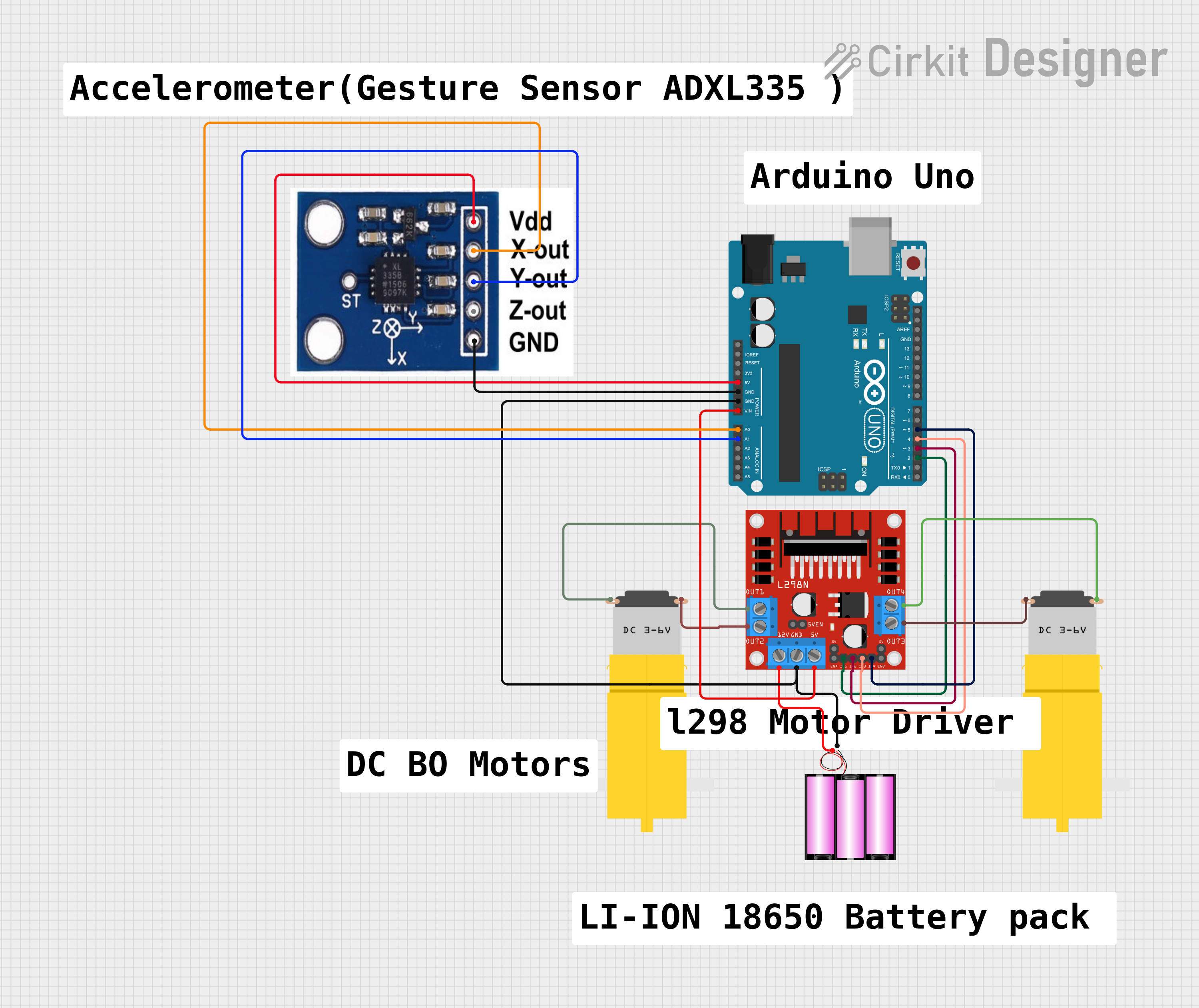 Open Project in Cirkit Designer
Explore Projects Built with AD7302
Open Project in Cirkit DesignerOpen Project in Cirkit DesignerOpen Project in Cirkit DesignerOpen Project in Cirkit DesignerCommon Applications
- Audio signal processing
- Industrial control systems
- Data acquisition systems
- Instrumentation and measurement devices
- Portable and battery-powered devices
Technical Specifications
The following table outlines the key technical specifications of the AD7302:
| Parameter | Value |
|---|---|
| Resolution | 12 bits |
| Number of DAC Channels | 2 |
| Supply Voltage Range | 2.7 V to 5.5 V |
| Power Consumption | 1.5 mW (typical at 3 V supply) |
| Output Voltage Range | 0 V to VREF |
| Reference Voltage (VREF) | 2.5 V (typical) |
| Interface Type | Serial (SPI-compatible) |
| Maximum Update Rate | 1 MSPS |
| Operating Temperature Range | -40°C to +85°C |
| Package Options | 8-lead SOIC, 8-lead TSSOP |
Pin Configuration and Descriptions
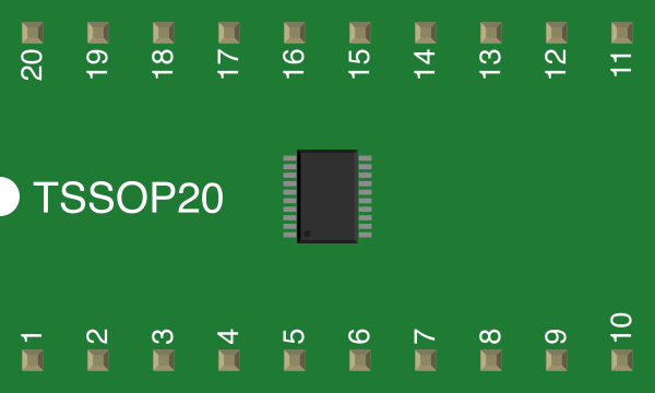
The AD7302 is available in an 8-lead SOIC or TSSOP package. The pin configuration and descriptions are as follows:
| Pin Number | Pin Name | Description |
|---|---|---|
| 1 | VDD | Positive power supply (2.7 V to 5.5 V). |
| 2 | VOUTA | Analog output for DAC channel A. |
| 3 | VOUTB | Analog output for DAC channel B. |
| 4 | GND | Ground reference. |
| 5 | SYNC | Active-low chip select input for the serial interface. |
| 6 | SCLK | Serial clock input for the SPI-compatible interface. |
| 7 | DIN | Serial data input for the SPI-compatible interface. |
| 8 | VREF | Reference voltage input for both DAC channels. |
Usage Instructions
How to Use the AD7302 in a Circuit
- Power Supply: Connect the VDD pin to a stable power supply within the range of 2.7 V to 5.5 V. Connect the GND pin to the ground of the circuit.
- Reference Voltage: Provide a stable reference voltage (e.g., 2.5 V) to the VREF pin. This determines the output voltage range of the DAC.
- Serial Interface: Use the SPI-compatible interface to send data to the DAC:
- Connect the SYNC pin to a GPIO pin on your microcontroller to act as a chip select.
- Connect the SCLK pin to the SPI clock line.
- Connect the DIN pin to the SPI data output line of your microcontroller.
- Outputs: Connect the VOUTA and VOUTB pins to the desired analog loads or circuits.
Important Considerations
- Ensure that the reference voltage (VREF) is stable and noise-free for accurate DAC performance.
- Use decoupling capacitors (e.g., 0.1 µF) close to the VDD and VREF pins to minimize power supply noise.
- The SYNC pin must be pulled low to enable communication with the device. Data is latched on the rising edge of SYNC.
- The maximum SPI clock frequency should not exceed the specified limits in the datasheet.
Example Code for Arduino UNO
Below is an example of how to interface the AD7302 with an Arduino UNO using the SPI library:
#include <SPI.h>

// Define pin connections
const int SYNC_PIN = 10; // Chip select pin for AD7302

void setup() {
  // Initialize SPI communication
  SPI.begin();
  SPI.setClockDivider(SPI_CLOCK_DIV16); // Set SPI clock speed
  SPI.setDataMode(SPI_MODE2);           // SPI mode 2 for AD7302
  pinMode(SYNC_PIN, OUTPUT);            // Set SYNC pin as output
  digitalWrite(SYNC_PIN, HIGH);         // Set SYNC pin high (inactive)
}

void loop() {
  // Example: Set DAC channel A to mid-scale (2048 out of 4096)
  uint16_t dacValue = 2048; // 12-bit value for DAC
  writeDAC(0, dacValue);    // Write to channel A
  delay(1000);              // Wait for 1 second
}

// Function to write data to the AD7302
void writeDAC(uint8_t channel, uint16_t value) {
  // Ensure value is 12-bit
  value &= 0x0FFF;

  // Construct the 16-bit data word
  uint16_t dataWord = (channel << 15) | (value & 0x0FFF);

  // Send data to AD7302
  digitalWrite(SYNC_PIN, LOW);          // Activate SYNC (chip select)
  SPI.transfer(highByte(dataWord));     // Send high byte
  SPI.transfer(lowByte(dataWord));      // Send low byte
  digitalWrite(SYNC_PIN, HIGH);         // Deactivate SYNC
}
Notes:
- The
channelparameter in thewriteDACfunction should be0for channel A and1for channel B. - Ensure that the SPI clock speed does not exceed the maximum supported by the AD7302.
Troubleshooting and FAQs
Common Issues
No Output Signal:
- Verify that the power supply (VDD) and ground (GND) connections are correct.
- Ensure that the reference voltage (VREF) is applied and stable.
- Check the SPI connections and ensure the SYNC pin is toggled correctly.
Incorrect Output Voltage:
- Confirm that the data sent to the DAC is in the correct 12-bit format.
- Verify that the reference voltage matches the expected value.
- Check for noise or instability in the power supply or reference voltage.
Communication Failure:
- Ensure the SPI clock speed and mode (SPI_MODE2) are correctly configured.
- Verify that the SYNC pin is pulled low during data transmission.
FAQs
Q1: Can the AD7302 operate with a 5 V power supply?
Yes, the AD7302 supports a supply voltage range of 2.7 V to 5.5 V.
Q2: What is the maximum output voltage of the DAC?
The maximum output voltage is determined by the reference voltage (VREF). For example, if VREF is 2.5 V, the output voltage range is 0 V to 2.5 V.
Q3: Can I use the AD7302 with a microcontroller that does not support SPI?
Yes, you can implement a bit-banging SPI protocol using GPIO pins, but this may require additional coding effort.
Q4: How do I ensure accurate DAC performance?
Use a stable and low-noise reference voltage, and place decoupling capacitors close to the VDD and VREF pins.