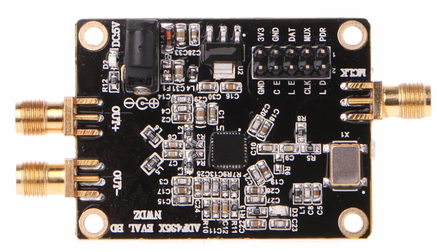
How to Use ADF4351: Examples, Pinouts, and Specs
Introduction
The ADF4351, manufactured by Analog Devices, is a wideband frequency synthesizer capable of generating frequencies from 137.5 MHz to 4.4 GHz. It combines a high-performance phase-locked loop (PLL) with an integrated voltage-controlled oscillator (VCO), offering low phase noise and high frequency resolution. The ADF4351 is highly versatile and can be used in a variety of applications, including:
- Wireless communication systems (e.g., GSM, LTE, Wi-Fi)
- Radar systems
- Signal generation and test equipment
- Satellite communication
- Instrumentation and measurement systems
Its ability to generate a wide range of frequencies with fine resolution makes it a popular choice for engineers and designers working on RF and microwave systems.
Explore Projects Built with ADF4351

Explore Projects Built with ADF4351
Technical Specifications
Key Technical Details
- Frequency Range: 137.5 MHz to 4.4 GHz
- Phase Noise: Low phase noise performance
- Frequency Resolution: Programmable down to 0.1 Hz
- Power Supply Voltage: 3.0 V to 3.6 V
- Current Consumption: ~30 mA (typical, depending on configuration)
- Output Power Levels: Programmable in 4 steps (-4 dBm to +5 dBm)
- Reference Input Frequency: Up to 250 MHz
- Phase Detector Frequency: Up to 125 MHz
- Lock Time: Fast lock capability
- Interface: 3-wire SPI (Serial Peripheral Interface)
- Operating Temperature Range: -40°C to +85°C
Pin Configuration and Descriptions
The ADF4351 is available in a 32-lead LFCSP (Lead Frame Chip Scale Package). Below is the pin configuration and description:
| Pin Number | Pin Name | Description |
|---|---|---|
| 1 | VREF | Reference voltage for the charge pump. |
| 2 | RSET | External resistor to set charge pump current. |
| 3 | CP | Charge pump output. Connect to the loop filter. |
| 4 | VDD | Power supply for the PLL circuitry. |
| 5 | GND | Ground connection. |
| 6 | RFOUTA+ | Positive RF output. |
| 7 | RFOUTA- | Negative RF output. |
| 8 | RFOUTB | Auxiliary RF output. |
| 9 | VCO | Voltage-controlled oscillator supply. |
| 10 | VTUNE | Control voltage input for the VCO. |
| 11 | CE | Chip enable. Active high. |
| 12 | CLK | SPI clock input. |
| 13 | DATA | SPI data input. |
| 14 | LE | SPI latch enable. |
| 15 | GND | Ground connection. |
| 16 | REFIN | Reference input signal. |
| 17-32 | NC or GND | Not connected or ground (depending on the specific pin). |
Refer to the ADF4351 datasheet for the complete pinout and PCB layout guidelines.
Usage Instructions
How to Use the ADF4351 in a Circuit
- Power Supply: Connect a stable 3.3 V power supply to the VDD and VCO pins. Ensure proper decoupling capacitors are placed close to the pins to minimize noise.
- Reference Input: Provide a clean reference clock signal to the REFIN pin. The frequency of this signal determines the phase detector frequency and overall frequency resolution.
- Loop Filter: Design and connect an appropriate loop filter between the CP (charge pump) pin and the VTUNE pin. The loop filter stabilizes the PLL and determines the lock time and phase noise performance.
- RF Outputs: Use the RFOUTA+ and RFOUTA- pins for the primary RF output. The RFOUTB pin can be used as an auxiliary output if needed.
- SPI Interface: Use a microcontroller or FPGA to program the ADF4351 via its 3-wire SPI interface (CLK, DATA, LE). Configure the frequency, output power, and other parameters by writing to the appropriate registers.
Important Considerations and Best Practices
- PCB Layout: Ensure a proper ground plane and minimize trace lengths for high-frequency signals to reduce noise and interference.
- Thermal Management: The ADF4351 can generate heat during operation. Use thermal vias and a heatsink if necessary.
- Programming: Follow the register map in the datasheet to configure the device. Incorrect programming can result in unstable operation or failure to lock.
- Output Matching: Match the RF output impedance (typically 50 ohms) to the load for optimal performance.
Example Code for Arduino UNO
Below is an example of how to program the ADF4351 using an Arduino UNO:
// ADF4351 SPI Control Example for Arduino UNO
// This code configures the ADF4351 to output a frequency of 1 GHz.
// Ensure proper connections: CLK -> D13, DATA -> D11, LE -> D10

#include <SPI.h>

#define LE_PIN 10  // Latch Enable pin connected to Arduino pin 10

void setup() {
  pinMode(LE_PIN, OUTPUT);
  digitalWrite(LE_PIN, HIGH);  // Set LE high initially
  SPI.begin();
  SPI.setDataMode(SPI_MODE0);  // SPI mode 0
  SPI.setClockDivider(SPI_CLOCK_DIV16);  // Set SPI clock speed
}

void loop() {
  // Example: Write to ADF4351 registers
  writeRegister(0x00580001);  // Register 0: Set frequency and other parameters
  writeRegister(0x08000042);  // Register 1: PLL settings
  writeRegister(0x000004B3);  // Register 2: Charge pump and phase detector
  writeRegister(0x0000000B);  // Register 3: Reference divider and R counter
  writeRegister(0x00C00005);  // Register 4: Output power and RF settings
  writeRegister(0x00400000);  // Register 5: Power-down and other settings

  delay(1000);  // Wait for 1 second before reprogramming (if needed)
}

void writeRegister(uint32_t data) {
  digitalWrite(LE_PIN, LOW);  // Set LE low to start transmission
  SPI.transfer((data >> 24) & 0xFF);  // Send MSB first
  SPI.transfer((data >> 16) & 0xFF);
  SPI.transfer((data >> 8) & 0xFF);
  SPI.transfer(data & 0xFF);  // Send LSB last
  digitalWrite(LE_PIN, HIGH);  // Set LE high to latch the data
}
Notes:
- Replace the register values in the example code with the appropriate values for your application.
- Consult the ADF4351 datasheet for detailed register descriptions and programming examples.
Troubleshooting and FAQs
Common Issues and Solutions
PLL Fails to Lock:
- Verify the reference input signal is clean and within the specified frequency range.
- Check the loop filter design and ensure it matches the desired frequency range and phase noise requirements.
- Confirm that the SPI programming sequence is correct and all registers are configured properly.
No RF Output:
- Ensure the RFOUTA+ and RFOUTA- pins are properly connected to the load.
- Check the output power settings in the register configuration.
- Verify that the chip is enabled (CE pin is high).
High Phase Noise:
- Use a low-jitter reference clock for the REFIN pin.
- Optimize the loop filter design for the desired phase noise performance.
- Minimize noise on the power supply by using proper decoupling capacitors.
Overheating:
- Ensure proper thermal management, such as using a heatsink or thermal vias.
- Reduce the output power level if possible.
FAQs
Can the ADF4351 generate frequencies below 137.5 MHz? No, the ADF4351 is designed to operate within the range of 137.5 MHz to 4.4 GHz. For lower frequencies, consider using a frequency divider or a different synthesizer.
What is the maximum SPI clock speed? The ADF4351 supports SPI clock speeds up to 20 MHz.
Can I use the ADF4351 with a 5V microcontroller? Yes, but you must use level shifters to interface the 5V logic levels with the 3.3V SPI pins of the ADF4351.
For further details, refer to the official ADF4351 datasheet and application notes provided by Analog Devices.