How to Use MUX ADG708: Examples, Pinouts, and Specs
Introduction
The ADG708 is a low on-resistance, dual 4-channel multiplexer/demultiplexer manufactured by Analog Devices. It is designed for switching analog signals with minimal distortion and high-speed operation. The device is ideal for applications requiring precise signal routing, such as audio, video, and data communication systems. Its low on-resistance and high linearity make it suitable for high-performance analog signal processing.
Explore Projects Built with MUX ADG708
Explore Projects Built with MUX ADG708
Common Applications
- Audio and video signal routing
- Data acquisition systems
- Communication systems
- Test and measurement equipment
- Industrial control systems
Technical Specifications
Key Technical Details
- Supply Voltage (VDD): 2.7 V to 5.5 V
- On-Resistance (RON): 2.5 Ω (typical at 5 V)
- On-Resistance Flatness: 0.5 Ω (typical at 5 V)
- Switching Time: 20 ns (typical at 5 V)
- Bandwidth: 200 MHz
- Power Consumption: 0.01 µW (typical in standby mode)
- Operating Temperature Range: -40°C to +85°C
- ESD Protection: 2 kV (HBM)
Pin Configuration and Descriptions
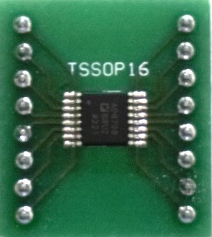
The ADG708 is available in a 16-lead TSSOP or LFCSP package. Below is the pin configuration and description:
| Pin Number | Pin Name | Description |
|---|---|---|
| 1 | S1A | Source 1 for channel A |
| 2 | S2A | Source 2 for channel A |
| 3 | S3A | Source 3 for channel A |
| 4 | S4A | Source 4 for channel A |
| 5 | D1 | Drain for channel A |
| 6 | VSS | Ground (0 V reference) |
| 7 | IN1 | Logic control input for channel selection |
| 8 | IN2 | Logic control input for channel selection |
| 9 | EN | Enable pin (active low) |
| 10 | VDD | Positive supply voltage |
| 11 | D2 | Drain for channel B |
| 12 | S4B | Source 4 for channel B |
| 13 | S3B | Source 3 for channel B |
| 14 | S2B | Source 2 for channel B |
| 15 | S1B | Source 1 for channel B |
| 16 | NC | No connection |
Usage Instructions
How to Use the ADG708 in a Circuit
Power Supply:
- Connect the VDD pin to a power supply within the range of 2.7 V to 5.5 V.
- Connect the VSS pin to ground (0 V reference).
Channel Selection:
- Use the IN1 and IN2 pins to select the active channel. The logic levels are as follows:
- IN1 = 0, IN2 = 0: Channel 1 selected
- IN1 = 0, IN2 = 1: Channel 2 selected
- IN1 = 1, IN2 = 0: Channel 3 selected
- IN1 = 1, IN2 = 1: Channel 4 selected
- Use the IN1 and IN2 pins to select the active channel. The logic levels are as follows:
Enable/Disable:
- The EN pin is active low. Pull it low to enable the multiplexer. Pull it high to disable all channels.
Signal Routing:
- Connect the analog signals to the S1A–S4A or S1B–S4B pins.
- The selected signal will be routed to the corresponding drain pin (D1 or D2).
Decoupling Capacitor:
- Place a 0.1 µF decoupling capacitor close to the VDD pin to reduce noise and improve stability.
Example: Connecting the ADG708 to an Arduino UNO
The ADG708 can be controlled using an Arduino UNO to select channels and route signals. Below is an example code snippet:
// Define control pins for ADG708
const int IN1 = 2;  // Connect to Arduino digital pin 2
const int IN2 = 3;  // Connect to Arduino digital pin 3
const int EN = 4;   // Connect to Arduino digital pin 4

void setup() {
  // Set control pins as outputs
  pinMode(IN1, OUTPUT);
  pinMode(IN2, OUTPUT);
  pinMode(EN, OUTPUT);

  // Enable the ADG708
  digitalWrite(EN, LOW);  // Active low enable
}

void loop() {
  // Select Channel 1
  digitalWrite(IN1, LOW);
  digitalWrite(IN2, LOW);
  delay(1000);  // Wait for 1 second

  // Select Channel 2
  digitalWrite(IN1, LOW);
  digitalWrite(IN2, HIGH);
  delay(1000);  // Wait for 1 second

  // Select Channel 3
  digitalWrite(IN1, HIGH);
  digitalWrite(IN2, LOW);
  delay(1000);  // Wait for 1 second

  // Select Channel 4
  digitalWrite(IN1, HIGH);
  digitalWrite(IN2, HIGH);
  delay(1000);  // Wait for 1 second
}
Important Considerations
- Ensure the input signals are within the supply voltage range to avoid damage.
- Use proper decoupling capacitors to minimize noise.
- Avoid leaving unused pins floating; connect them to ground or a defined logic level.
Troubleshooting and FAQs
Common Issues and Solutions
No Signal Output:
- Verify that the EN pin is pulled low to enable the device.
- Check the logic levels on IN1 and IN2 to ensure the correct channel is selected.
High Signal Distortion:
- Ensure the input signal amplitude is within the specified range.
- Check for proper grounding and minimize noise in the circuit.
Device Overheating:
- Verify that the supply voltage does not exceed 5.5 V.
- Ensure the load connected to the drain pins does not exceed the current rating.
Unexpected Behavior:
- Check for loose connections or soldering issues.
- Confirm that unused pins are not left floating.
FAQs
Q: Can the ADG708 handle digital signals?
A: Yes, the ADG708 can switch both analog and digital signals, provided they are within the supply voltage range.
Q: What is the maximum signal frequency the ADG708 can handle?
A: The ADG708 has a bandwidth of 200 MHz, making it suitable for high-frequency signals.
Q: Can I use the ADG708 with a 3.3 V microcontroller?
A: Yes, the ADG708 operates with supply voltages as low as 2.7 V, making it compatible with 3.3 V systems.
Q: How do I reduce crosstalk between channels?
A: Use proper PCB layout techniques, such as separating signal traces and using ground planes, to minimize crosstalk.