
How to Use SHIFT REGISTER: Examples, Pinouts, and Specs

 Design with SHIFT REGISTER in Cirkit Designer
Introduction
A shift register is a sequential circuit designed to store and manipulate binary data. It consists of a series of flip-flops connected in a chain, enabling data to be shifted in or out serially. This functionality makes shift registers highly versatile for applications such as data storage, data transfer, and conversion between serial and parallel formats.
Explore Projects Built with SHIFT REGISTER
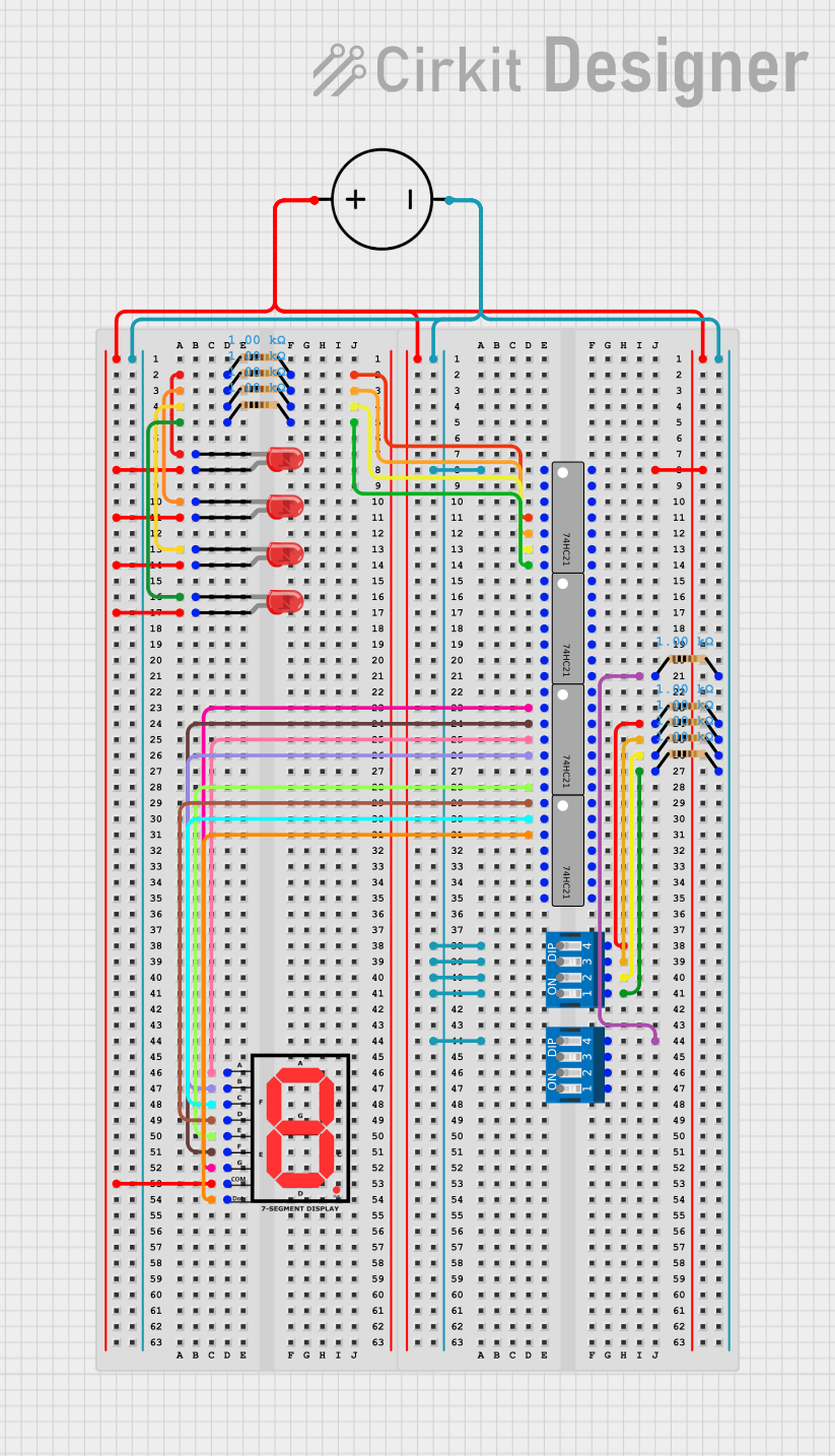 Open Project in Cirkit Designer
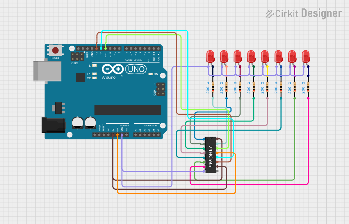 Open Project in Cirkit Designer
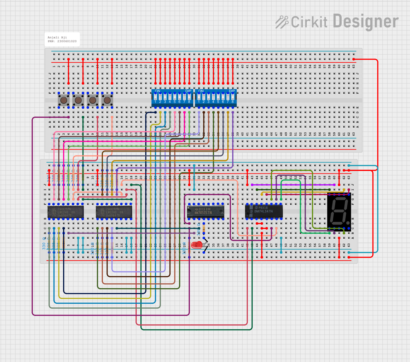 Open Project in Cirkit Designer
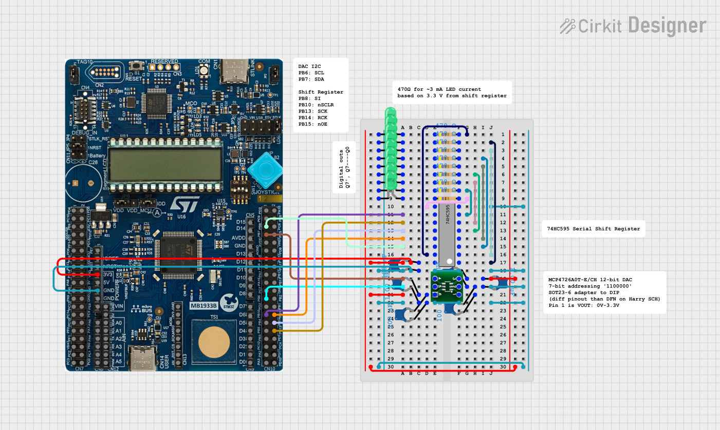 Open Project in Cirkit Designer
Explore Projects Built with SHIFT REGISTER
Open Project in Cirkit DesignerOpen Project in Cirkit DesignerOpen Project in Cirkit DesignerOpen Project in Cirkit DesignerCommon Applications and Use Cases:
- Expanding the number of output pins in microcontrollers (e.g., Arduino).
- Serial-to-parallel or parallel-to-serial data conversion.
- LED matrix control and display systems.
- Digital signal processing and data buffering.
- Memory storage in digital circuits.
Technical Specifications
Below are the general technical specifications for a commonly used shift register, the 74HC595:
Key Technical Details:
- Operating Voltage (Vcc): 2V to 6V.
- Maximum Clock Frequency: 25 MHz (at 5V).
- Output Current (per pin): 6 mA (max).
- Power Dissipation: 500 mW (max).
- Number of Output Pins: 8 (parallel outputs).
- Serial Data Input: 1 pin (DS).
- Clock Input: 1 pin (SH_CP).
- Latch Input: 1 pin (ST_CP).
Pin Configuration and Descriptions:
| Pin Number | Pin Name | Description |
|---|---|---|
| 1 | Q1 | Parallel output pin 1. |
| 2 | Q2 | Parallel output pin 2. |
| 3 | Q3 | Parallel output pin 3. |
| 4 | Q4 | Parallel output pin 4. |
| 5 | Q5 | Parallel output pin 5. |
| 6 | Q6 | Parallel output pin 6. |
| 7 | Q7 | Parallel output pin 7. |
| 8 | GND | Ground pin. Connect to circuit ground. |
| 9 | Q7' | Serial data output for cascading multiple shift registers. |
| 10 | MR | Master reset (active low). Clears all outputs when pulled low. |
| 11 | SH_CP | Shift register clock input. Data is shifted on the rising edge of this clock. |
| 12 | ST_CP | Storage register clock input (latch). Transfers data to output pins on rising edge. |
| 13 | OE | Output enable (active low). Enables/disables outputs without affecting data. |
| 14 | DS | Serial data input. |
| 15 | Q0 | Parallel output pin 0. |
| 16 | Vcc | Supply voltage. Connect to the positive terminal of the power supply. |
Usage Instructions
How to Use the Component in a Circuit:
Power Connections:
- Connect the Vcc pin to the positive terminal of your power supply (e.g., 5V).
- Connect the GND pin to the ground of your circuit.
Data Input:
- Use the DS pin to input serial data into the shift register.
Clock Signals:
- Provide a clock signal to the SH_CP pin to shift data into the register.
- Use the ST_CP pin to latch the data into the output pins.
Output Enable:
- Pull the OE pin low to enable the outputs. If left high, the outputs will be disabled.
Cascading Multiple Registers:
- Connect the Q7' pin of the first shift register to the DS pin of the next register.
- Share the same clock and latch signals across all registers.
Important Considerations and Best Practices:
- Use decoupling capacitors (e.g., 0.1 µF) near the Vcc pin to stabilize the power supply.
- Avoid exceeding the maximum current rating of the output pins to prevent damage.
- Ensure proper timing between the clock and latch signals to avoid data corruption.
- For cascading, ensure the clock frequency is appropriate for the number of registers used.
Example: Using the 74HC595 with an Arduino UNO
Below is an example of controlling 8 LEDs using a 74HC595 shift register and an Arduino UNO:
// Define pin connections
const int dataPin = 2;  // DS pin of 74HC595 connected to Arduino pin 2
const int clockPin = 3; // SH_CP pin of 74HC595 connected to Arduino pin 3
const int latchPin = 4; // ST_CP pin of 74HC595 connected to Arduino pin 4

void setup() {
  // Set pin modes
  pinMode(dataPin, OUTPUT);
  pinMode(clockPin, OUTPUT);
  pinMode(latchPin, OUTPUT);
}

void loop() {
  // Example pattern to display on LEDs
  byte ledPattern = 0b10101010; // Binary pattern for LEDs (on/off)

  // Send data to the shift register
  digitalWrite(latchPin, LOW); // Disable latch to load data
  shiftOut(dataPin, clockPin, MSBFIRST, ledPattern); // Shift data
  digitalWrite(latchPin, HIGH); // Enable latch to display data

  delay(500); // Wait for 500ms
}
Explanation of the Code:
shiftOut(): Sends 8 bits of data to the shift register, one bit at a time.- Latch Control: The latch pin is toggled to transfer the shifted data to the output pins.
- LED Pattern: The binary value
0b10101010turns on alternate LEDs.
Troubleshooting and FAQs
Common Issues and Solutions:
No Output on LEDs:
- Ensure the OE pin is connected to ground (active low).
- Verify the power supply connections to Vcc and GND.
Incorrect LED Pattern:
- Check the timing of the clock and latch signals.
- Ensure the data sent matches the desired output pattern.
Cascaded Registers Not Working:
- Verify the connection between the Q7' pin of the first register and the DS pin of the next.
- Ensure all registers share the same clock and latch signals.
Overheating or Damage:
- Avoid exceeding the maximum current rating of the output pins.
- Use current-limiting resistors for LEDs or other loads.
FAQs:
Q: Can I use the 74HC595 with 3.3V logic?
- A: Yes, the 74HC595 is compatible with 3.3V logic, but ensure the supply voltage is within the operating range (2V to 6V).
Q: How many shift registers can I cascade?
- A: Theoretically, you can cascade as many as needed, but practical limitations include clock frequency, signal integrity, and power supply capacity.
Q: What is the purpose of the OE pin?
- A: The OE pin allows you to enable or disable the outputs without affecting the stored data.
By following this documentation, you can effectively use a shift register like the 74HC595 in your projects!