How to Use 74hc165: Examples, Pinouts, and Specs
Introduction
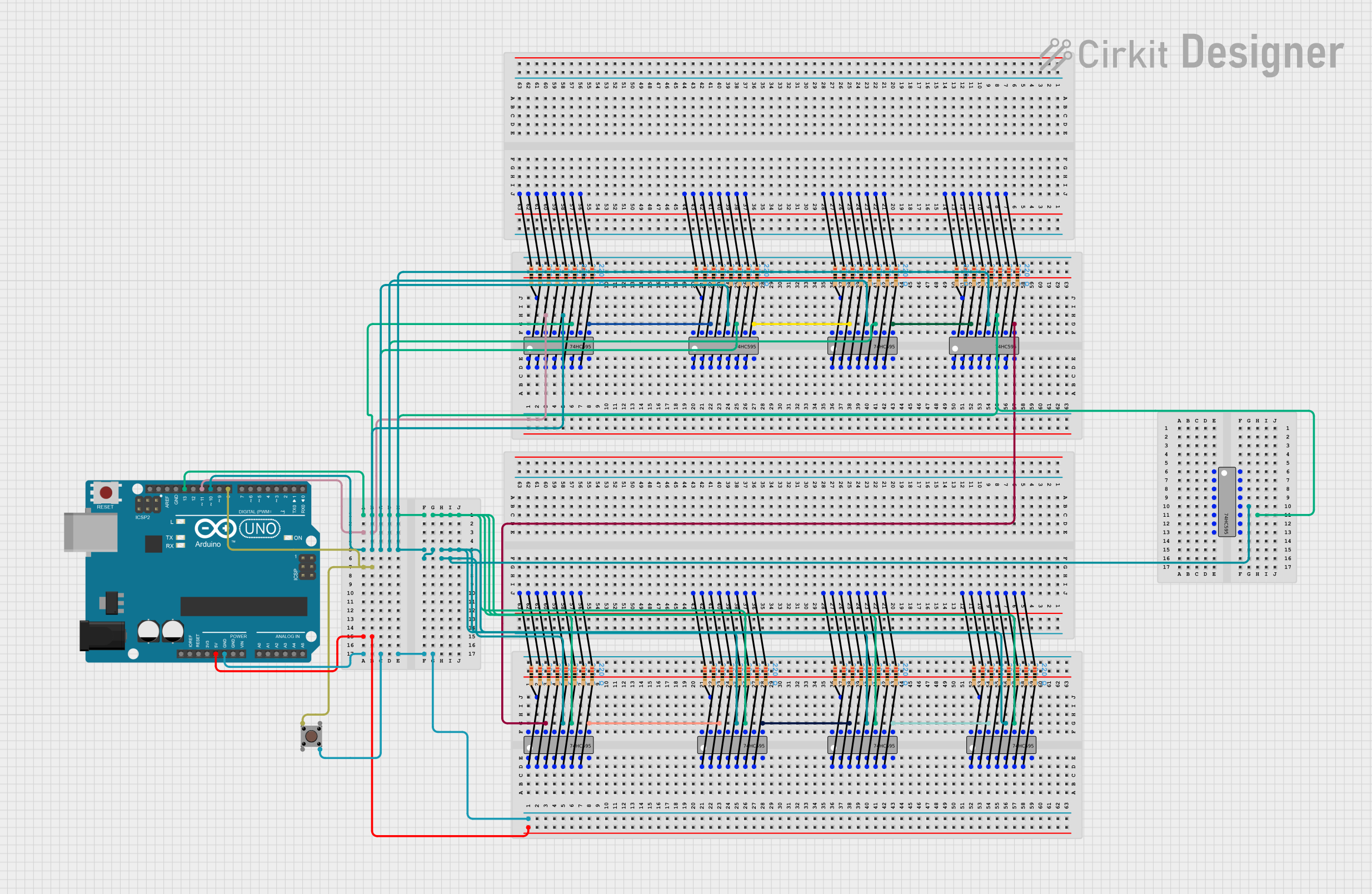
The 74HC165 is an 8-bit parallel-in/serial-out shift register. It allows for the parallel loading of data and serial output, making it useful for converting parallel data into a serial format for easier transmission or processing. This component is widely used in digital electronics for expanding input capabilities, interfacing with microcontrollers, and reducing the number of I/O pins required for data acquisition.
Explore Projects Built with 74hc165
Explore Projects Built with 74hc165
Common Applications and Use Cases
- Expanding the number of input pins for microcontrollers
- Reading multiple switches or sensors in parallel
- Serial communication of parallel data
- Data acquisition systems
- Digital signal processing
Technical Specifications
The 74HC165 is a high-speed CMOS device that operates with low power consumption. Below are its key technical details:
| Parameter | Value |
|---|---|
| Supply Voltage (Vcc) | 2V to 6V |
| Input Voltage Range | 0V to Vcc |
| Maximum Clock Frequency | 29 MHz (at Vcc = 5V) |
| Output Current (per pin) | ±6 mA |
| Operating Temperature | -40°C to +125°C |
| Propagation Delay | ~13 ns (at Vcc = 5V) |
| Package Types | DIP-16, SOIC-16, TSSOP-16 |
Pin Configuration and Descriptions
The 74HC165 has 16 pins, as described in the table below:
| Pin Number | Pin Name | Description |
|---|---|---|
| 1 | Q7 | Serial data output (MSB) |
| 2 | CP (Clock) | Clock input for shifting data |
| 3 | CE (Enable) | Active-low clock enable input |
| 4 | D4 | Parallel data input (bit 4) |
| 5 | D5 | Parallel data input (bit 5) |
| 6 | D6 | Parallel data input (bit 6) |
| 7 | D7 | Parallel data input (bit 7) |
| 8 | GND | Ground (0V) |
| 9 | D3 | Parallel data input (bit 3) |
| 10 | D2 | Parallel data input (bit 2) |
| 11 | D1 | Parallel data input (bit 1) |
| 12 | D0 | Parallel data input (bit 0) |
| 13 | PL (Load) | Active-low parallel load input |
| 14 | Q7' | Complementary serial data output (used for cascading multiple 74HC165 devices) |
| 15 | Vcc | Positive supply voltage |
| 16 | SH/LD | Shift/Load control input (active-low) |
Usage Instructions
The 74HC165 is commonly used to read multiple parallel inputs and send the data serially to a microcontroller. Below are the steps to use the component in a circuit:
Circuit Connection
- Connect the Vcc pin to the positive supply voltage (e.g., 5V) and the GND pin to ground.
- Connect the parallel data inputs (D0 to D7) to the switches, sensors, or other devices you want to read.
- Use the PL (Load) pin to load the parallel data into the shift register. This pin is active-low, so it must be pulled low momentarily to load the data.
- Use the CP (Clock) pin to shift the data serially. Each clock pulse shifts one bit of data to the Q7 output.
- The CE pin must be held low to enable the clock. If this pin is high, the clock is disabled.
- The SH/LD pin determines whether the device is in shift mode (high) or load mode (low).
Example Arduino Code
The following example demonstrates how to use the 74HC165 with an Arduino UNO to read 8 parallel inputs and display the data in the Serial Monitor.
// Pin definitions
const int loadPin = 8;  // Connect to PL (Pin 13) of 74HC165
const int clockPin = 9; // Connect to CP (Pin 2) of 74HC165
const int dataPin = 10; // Connect to Q7 (Pin 1) of 74HC165

void setup() {
  pinMode(loadPin, OUTPUT);
  pinMode(clockPin, OUTPUT);
  pinMode(dataPin, INPUT);
  Serial.begin(9600); // Initialize Serial Monitor
}

void loop() {
  digitalWrite(loadPin, LOW);  // Load parallel data into the shift register
  delayMicroseconds(5);       // Small delay for stability
  digitalWrite(loadPin, HIGH); // Return to shift mode

  byte inputData = 0; // Variable to store the shifted data

  for (int i = 0; i < 8; i++) {
    digitalWrite(clockPin, LOW); // Generate a clock pulse
    delayMicroseconds(5);
    inputData |= (digitalRead(dataPin) << (7 - i)); // Read data bit by bit
    digitalWrite(clockPin, HIGH);
    delayMicroseconds(5);
  }

  Serial.print("Input Data: ");
  Serial.println(inputData, BIN); // Print the data in binary format
  delay(500); // Wait before the next read
}
Important Considerations and Best Practices
- Use pull-up or pull-down resistors on the parallel input pins (D0 to D7) to ensure stable readings when the inputs are not connected.
- Keep the clock signal clean and free of noise to avoid data corruption.
- If cascading multiple 74HC165 devices, connect the Q7' pin of the first device to the DS (serial input) pin of the next device.
Troubleshooting and FAQs
Common Issues
No data output on Q7 pin:
- Ensure the CE pin is held low to enable the clock.
- Verify that the PL pin is momentarily pulled low to load the parallel data.
Incorrect or unstable data:
- Check for noise on the clock signal or loose connections.
- Use pull-up or pull-down resistors on the parallel input pins.
Data not shifting properly:
- Confirm that the SH/LD pin is set high for shift mode.
- Verify the clock signal timing and ensure it meets the device's specifications.
FAQs
Q: Can I cascade multiple 74HC165 devices?
A: Yes, you can cascade multiple 74HC165 devices by connecting the Q7' pin of one device to the DS (serial input) pin of the next device. This allows you to read more than 8 inputs.
Q: What is the maximum clock frequency for the 74HC165?
A: The maximum clock frequency is 29 MHz when operating at a supply voltage of 5V.
Q: Can the 74HC165 be used with 3.3V systems?
A: Yes, the 74HC165 can operate with a supply voltage as low as 2V, making it compatible with 3.3V systems. Ensure that the input signals are within the voltage range of 0V to Vcc.