How to Use 74HC595 Shift Register: Examples, Pinouts, and Specs
Introduction
The 74HC595 is an 8-bit serial-in, parallel-out shift register manufactured by Texas Instruments. It is designed to expand the number of output pins available in microcontroller applications. By using a serial data input, the 74HC595 allows users to control up to 8 output pins with just 3 control pins from a microcontroller. This makes it ideal for applications where pin availability is limited.
Explore Projects Built with 74HC595 Shift Register
Explore Projects Built with 74HC595 Shift Register
Common Applications and Use Cases
- Driving multiple LEDs or 7-segment displays
- Expanding GPIO pins in microcontroller projects
- Controlling relays or other digital devices
- Data storage and transfer in digital systems
- Multiplexing and demultiplexing applications
Technical Specifications
The following are the key technical details of the 74HC595:
| Parameter | Value |
|---|---|
| Supply Voltage (Vcc) | 2V to 6V |
| Input Voltage Range | 0V to Vcc |
| Maximum Clock Frequency | 25 MHz (at 4.5V) |
| Output Current (per pin) | ±6 mA |
| Total Power Dissipation | 500 mW |
| Operating Temperature | -40°C to 125°C |
| Package Types | SOIC, PDIP, TSSOP, SSOP |
Pin Configuration and Descriptions
The 74HC595 has 16 pins, as described in the table below:
| Pin Number | Pin Name | Description |
|---|---|---|
| 1 | Q1 | Parallel output pin 1 |
| 2 | Q2 | Parallel output pin 2 |
| 3 | Q3 | Parallel output pin 3 |
| 4 | Q4 | Parallel output pin 4 |
| 5 | Q5 | Parallel output pin 5 |
| 6 | Q6 | Parallel output pin 6 |
| 7 | Q7 | Parallel output pin 7 |
| 8 | GND | Ground (0V) |
| 9 | Q7' | Serial data output for cascading multiple 74HC595 chips |
| 10 | MR | Master reset (active low) - clears all outputs |
| 11 | SH_CP | Shift register clock input - shifts data into the register on rising edge |
| 12 | ST_CP | Storage register clock input - transfers data to output pins on rising edge |
| 13 | OE | Output enable (active low) - enables/disables outputs |
| 14 | DS | Serial data input |
| 15 | Q0 | Parallel output pin 0 |
| 16 | Vcc | Supply voltage (2V to 6V) |
Usage Instructions
The 74HC595 is commonly used to expand the number of output pins in a circuit. Below are the steps and considerations for using the component:
Connecting the 74HC595
- Power Supply: Connect the Vcc pin (16) to a 5V or 3.3V power source and the GND pin (8) to ground.
- Control Pins:
- Connect the DS pin (14) to the microcontroller's data output pin.
- Connect the SH_CP pin (11) to the microcontroller's clock pin.
- Connect the ST_CP pin (12) to the microcontroller's latch pin.
- Outputs: Connect the Q0-Q7 pins (15, 1-7) to the devices you want to control (e.g., LEDs).
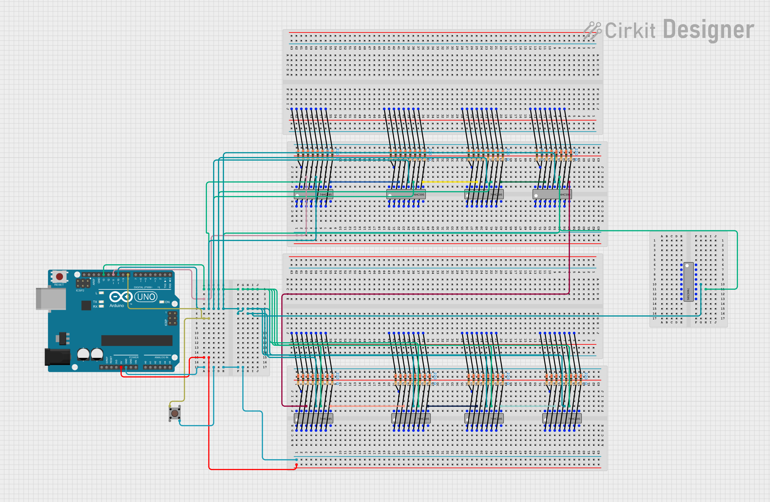
- Optional: If cascading multiple 74HC595 chips, connect the Q7' pin (9) of the first chip to the DS pin (14) of the next chip.
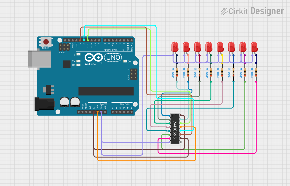
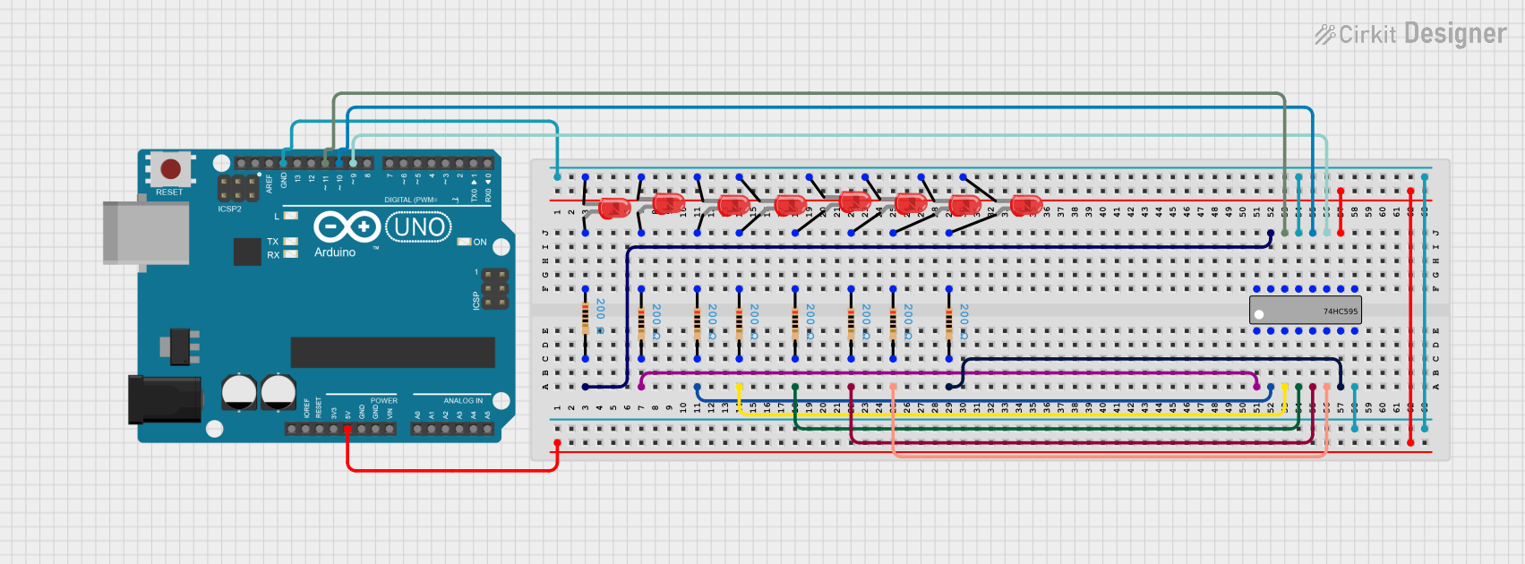
Example Circuit with Arduino UNO
Below is an example of how to connect and control the 74HC595 with an Arduino UNO to drive 8 LEDs:
Circuit Diagram
- Connect the DS pin to Arduino pin 11.
- Connect the SH_CP pin to Arduino pin 12.
- Connect the ST_CP pin to Arduino pin 8.
- Connect LEDs to Q0-Q7 with appropriate current-limiting resistors.
Arduino Code Example
// Define the control pins for the 74HC595
const int dataPin = 11;  // DS pin of 74HC595
const int clockPin = 12; // SH_CP pin of 74HC595
const int latchPin = 8;  // ST_CP pin of 74HC595

void setup() {
  // Set the control pins as outputs
  pinMode(dataPin, OUTPUT);
  pinMode(clockPin, OUTPUT);
  pinMode(latchPin, OUTPUT);
}

void loop() {
  // Example: Turn on LEDs in a binary counting pattern
  for (int i = 0; i < 256; i++) {
    digitalWrite(latchPin, LOW); // Prepare to send data
    shiftOut(dataPin, clockPin, MSBFIRST, i); // Send data to 74HC595
    digitalWrite(latchPin, HIGH); // Latch the data to output pins
    delay(500); // Wait for 500ms
  }
}
Important Considerations
- Use current-limiting resistors (e.g., 220Ω) for each LED to prevent excessive current draw.
- Ensure the total current drawn by all outputs does not exceed the chip's maximum rating.
- If cascading multiple chips, ensure the clock and latch signals are synchronized across all chips.
Troubleshooting and FAQs
Common Issues
- Outputs Not Responding:
- Check the connections to the control pins (DS, SH_CP, ST_CP).
- Ensure the OE pin is connected to ground (active low).
- Incorrect Output States:
- Verify the timing of the clock and latch signals.
- Ensure the data is shifted in the correct order (MSB or LSB first).
- Overheating:
- Check for excessive current draw on the output pins.
- Use appropriate resistors for connected devices.
FAQs
Q: Can I cascade multiple 74HC595 chips?
A: Yes, connect the Q7' pin of the first chip to the DS pin of the next chip. All chips share the same clock and latch signals.
Q: What is the purpose of the OE pin?
A: The OE (Output Enable) pin allows you to enable or disable all outputs simultaneously. It is active low, so connect it to ground to enable outputs.
Q: Can the 74HC595 drive high-power devices?
A: No, the 74HC595 is designed for low-power digital devices. Use a transistor or MOSFET to drive high-power devices.
By following this documentation, you can effectively use the 74HC595 shift register in your projects!