
How to Use SN74HCT74: Examples, Pinouts, and Specs
 Design with SN74HCT74 in Cirkit Designer
Introduction
The SN74HCT74 is a dual D-type flip-flop with set and reset inputs, manufactured by Texas Instruments. This component is designed for high-speed operation while maintaining low power consumption, making it ideal for a wide range of digital applications. Each flip-flop in the SN74HCT74 has independent data (D), clock (CLK), set (SET), and reset (RESET) inputs, as well as complementary outputs (Q and Q̅).
Explore Projects Built with SN74HCT74
 Open Project in Cirkit Designer
 Open Project in Cirkit Designer
 Open Project in Cirkit Designer
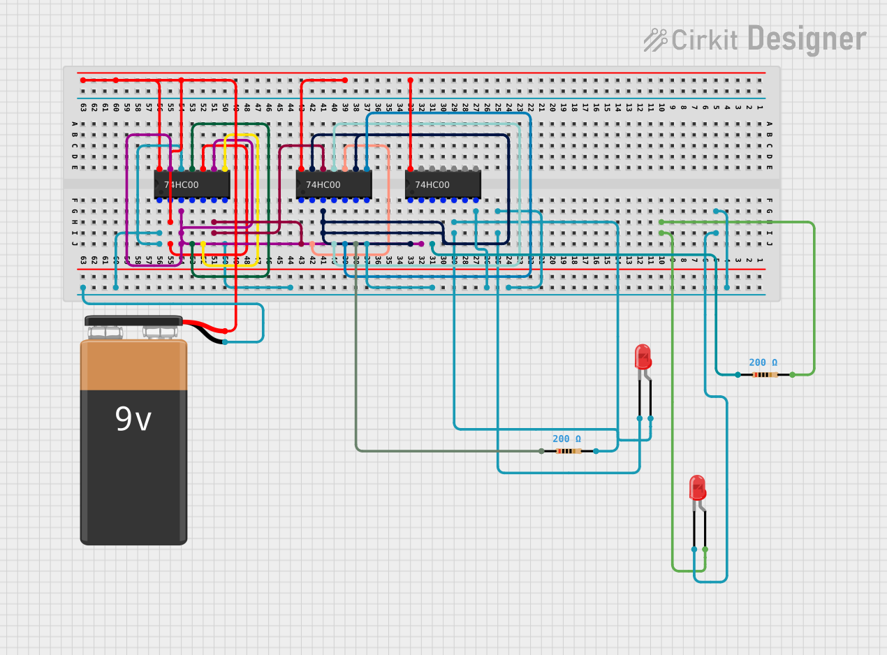 Open Project in Cirkit Designer
Explore Projects Built with SN74HCT74
Open Project in Cirkit DesignerOpen Project in Cirkit DesignerOpen Project in Cirkit DesignerOpen Project in Cirkit DesignerCommon Applications
- Data storage and synchronization in digital circuits
- Frequency division and clock signal generation
- Shift registers and counters
- Edge-triggered data latching in microcontroller-based systems
Technical Specifications
Key Technical Details
| Parameter | Value |
|---|---|
| Supply Voltage (Vcc) | 4.5 V to 5.5 V |
| Input Voltage Range | 0 V to Vcc |
| High-Level Input Voltage | 2.0 V (minimum) |
| Low-Level Input Voltage | 0.8 V (maximum) |
| Propagation Delay (typical) | 16 ns at 5 V |
| Output Current (I_O) | ±6 mA |
| Operating Temperature Range | -40°C to 85°C |
| Package Types | SOIC, PDIP, TSSOP, etc. |
Pin Configuration and Descriptions
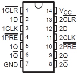
The SN74HCT74 is a 14-pin IC. Below is the pinout and description:
| Pin No. | Pin Name | Description |
|---|---|---|
| 1 | 1CLR̅ | Asynchronous clear (active low) for flip-flop 1 |
| 2 | 1D | Data input for flip-flop 1 |
| 3 | 1CLK | Clock input for flip-flop 1 |
| 4 | 1PRE̅ | Asynchronous preset (active low) for flip-flop 1 |
| 5 | 1Q | Output Q for flip-flop 1 |
| 6 | 1Q̅ | Complementary output Q̅ for flip-flop 1 |
| 7 | GND | Ground |
| 8 | 2Q̅ | Complementary output Q̅ for flip-flop 2 |
| 9 | 2Q | Output Q for flip-flop 2 |
| 10 | 2PRE̅ | Asynchronous preset (active low) for flip-flop 2 |
| 11 | 2CLK | Clock input for flip-flop 2 |
| 12 | 2D | Data input for flip-flop 2 |
| 13 | 2CLR̅ | Asynchronous clear (active low) for flip-flop 2 |
| 14 | Vcc | Positive power supply |
Usage Instructions
How to Use the SN74HCT74 in a Circuit
- Power Supply: Connect the Vcc pin (pin 14) to a 5 V power supply and the GND pin (pin 7) to ground.
- Data Input: Provide the data signal to the D input (pin 2 for flip-flop 1, pin 12 for flip-flop 2).
- Clock Signal: Apply a clock signal to the CLK input (pin 3 for flip-flop 1, pin 11 for flip-flop 2). The flip-flop captures the data on the rising edge of the clock.
- Set and Reset: Use the asynchronous SET (PRE̅) and CLEAR (CLR̅) inputs to force the outputs to a high or low state, respectively. These inputs are active low.
- Outputs: Monitor the Q and Q̅ outputs for the stored data (pins 5 and 6 for flip-flop 1, pins 9 and 8 for flip-flop 2).
Important Considerations
- Ensure that the input voltage levels are within the specified range to avoid damage to the IC.
- Use decoupling capacitors (e.g., 0.1 µF) near the Vcc pin to stabilize the power supply.
- Avoid floating inputs by connecting unused inputs to Vcc or GND through pull-up or pull-down resistors.
- The SET and RESET inputs override the clock and data inputs when activated.
Example: Using SN74HCT74 with Arduino UNO
The following example demonstrates how to use the SN74HCT74 to store and toggle a digital signal using an Arduino UNO.
// Example: Using SN74HCT74 with Arduino UNO
// This code toggles the state of a flip-flop using a clock signal from pin 8
// and a data signal from pin 7 of the Arduino.

const int clockPin = 8; // Arduino pin connected to SN74HCT74 clock input
const int dataPin = 7;  // Arduino pin connected to SN74HCT74 data input

void setup() {
  pinMode(clockPin, OUTPUT); // Set clock pin as output
  pinMode(dataPin, OUTPUT);  // Set data pin as output
}

void loop() {
  digitalWrite(dataPin, HIGH); // Set data input to HIGH
  digitalWrite(clockPin, HIGH); // Generate a rising edge on the clock
  delay(10);                   // Short delay
  digitalWrite(clockPin, LOW); // Set clock back to LOW
  delay(1000);                 // Wait for 1 second

  digitalWrite(dataPin, LOW);  // Set data input to LOW
  digitalWrite(clockPin, HIGH); // Generate another rising edge
  delay(10);                   // Short delay
  digitalWrite(clockPin, LOW); // Set clock back to LOW
  delay(1000);                 // Wait for 1 second
}
Troubleshooting and FAQs
Common Issues and Solutions
No Output on Q or Q̅:
- Ensure that the power supply is connected to Vcc and GND.
- Verify that the clock signal is being applied to the CLK pin.
- Check if the SET or RESET inputs are unintentionally activated.
Unexpected Behavior:
- Confirm that the input voltage levels are within the specified range.
- Ensure that unused inputs are not left floating.
High Power Consumption:
- Check for short circuits or incorrect wiring.
- Verify that the IC is operating within the recommended voltage range.
FAQs
Q1: Can I use the SN74HCT74 with a 3.3 V power supply?
A1: No, the SN74HCT74 requires a supply voltage between 4.5 V and 5.5 V. For 3.3 V systems, consider using a compatible IC.
Q2: What happens if both SET and RESET are activated simultaneously?
A2: Activating both SET and RESET simultaneously is not recommended, as it may lead to undefined behavior.
Q3: Can the SN74HCT74 be used for edge detection?
A3: Yes, the SN74HCT74 can be used for edge detection by leveraging its clock-triggered operation.