
How to Use W25Q128JV Module Header: Examples, Pinouts, and Specs

 Design with W25Q128JV Module Header in Cirkit Designer
Introduction
The W25Q128JV Module Header is a breakout board designed for the W25Q128JV flash memory chip. This module simplifies the integration of the W25Q128JV into electronic circuits by providing a convenient header interface. The W25Q128JV is a 128 Mbit (16 MB) serial flash memory chip that supports SPI (Serial Peripheral Interface) communication. It is widely used for data storage in embedded systems, IoT devices, and other applications requiring non-volatile memory.
Explore Projects Built with W25Q128JV Module Header
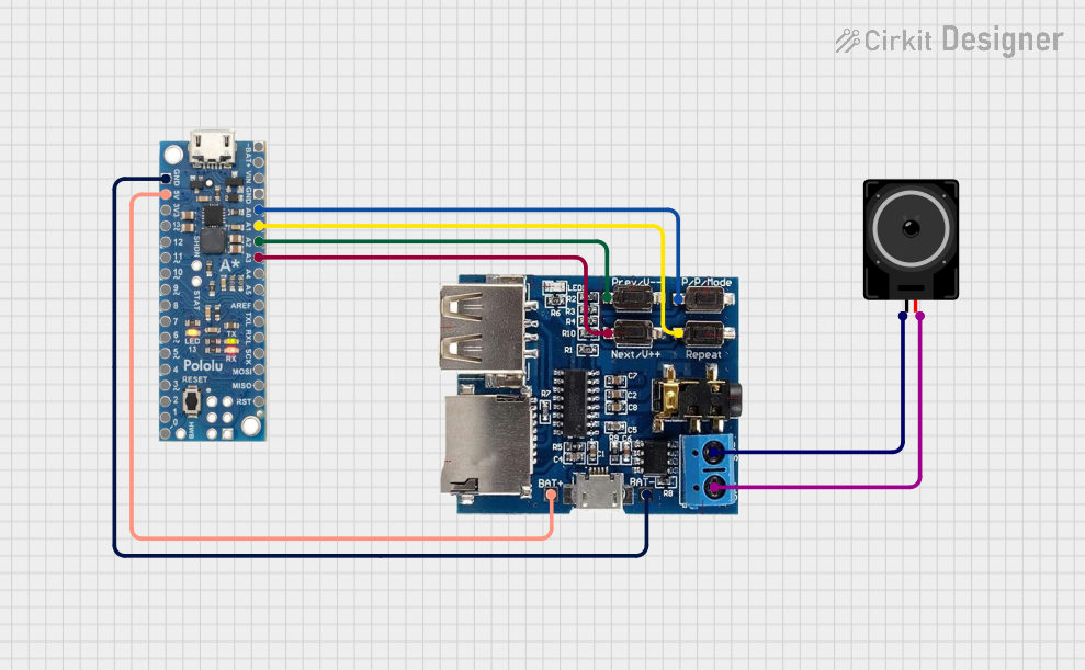 Open Project in Cirkit Designer
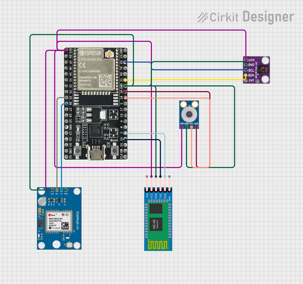 Open Project in Cirkit Designer
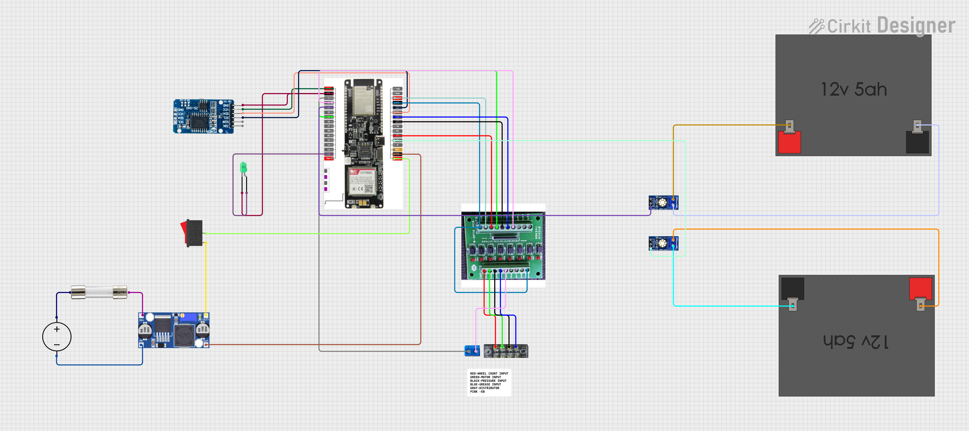 Open Project in Cirkit Designer
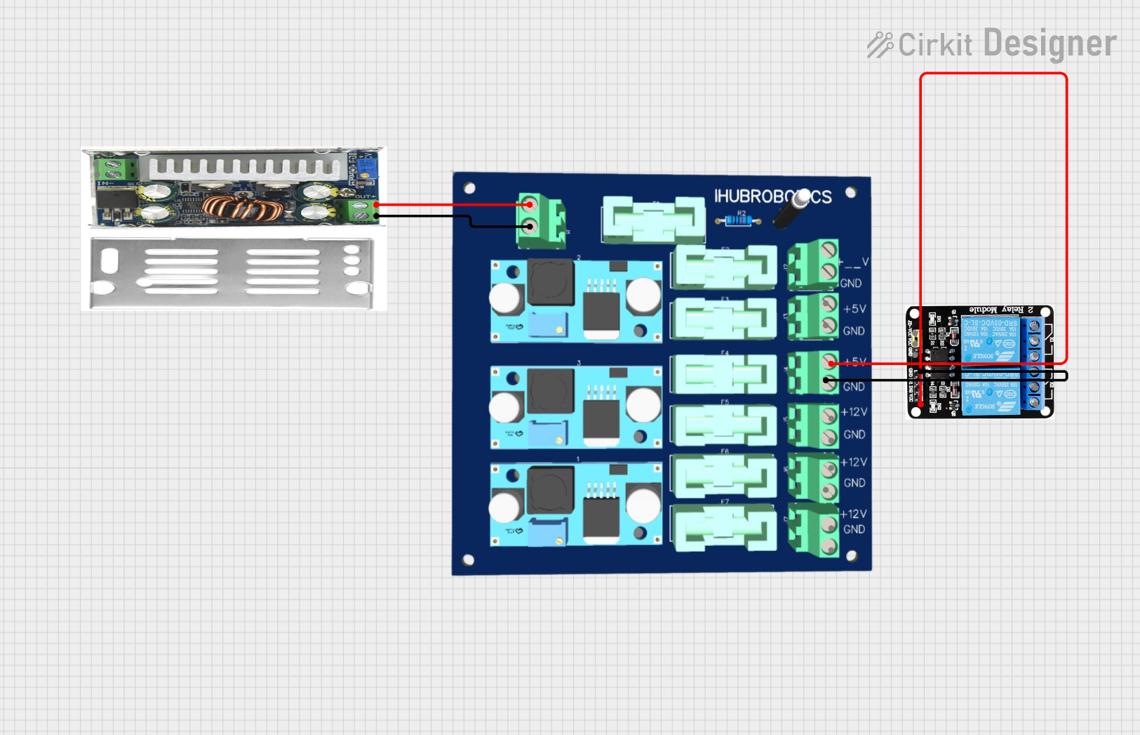 Open Project in Cirkit Designer
Explore Projects Built with W25Q128JV Module Header
Open Project in Cirkit DesignerOpen Project in Cirkit DesignerOpen Project in Cirkit DesignerOpen Project in Cirkit DesignerCommon Applications and Use Cases
- Firmware storage for microcontrollers and embedded systems
- Data logging in IoT devices
- Boot memory for systems requiring external flash
- Storage for multimedia files in portable devices
- General-purpose non-volatile memory for custom electronics projects
Technical Specifications
Key Technical Details
- Memory Capacity: 128 Mbit (16 MB)
- Interface: SPI (Serial Peripheral Interface)
- Operating Voltage: 2.7V to 3.6V
- Maximum Clock Frequency: 133 MHz
- Write/Erase Endurance: 100,000 cycles
- Data Retention: 20 years
- Operating Temperature: -40°C to +85°C
- Package: Module header with solderable pins for easy integration
Pin Configuration and Descriptions
The W25Q128JV Module Header exposes the following pins for connection:
| Pin Name | Pin Number | Description |
|---|---|---|
| VCC | 1 | Power supply input (2.7V to 3.6V). Connect to the 3.3V power rail. |
| GND | 2 | Ground connection. Connect to the circuit ground. |
| CS | 3 | Chip Select. Active low signal to enable communication with the module. |
| SCK | 4 | Serial Clock. Provides the clock signal for SPI communication. |
| MOSI | 5 | Master Out Slave In. Data input to the module from the microcontroller. |
| MISO | 6 | Master In Slave Out. Data output from the module to the microcontroller. |
| WP | 7 | Write Protect. Active low signal to protect the memory from write operations. |
| HOLD | 8 | Hold. Active low signal to pause communication without resetting the SPI bus. |
Usage Instructions
How to Use the Component in a Circuit
- Power Supply: Connect the
VCCpin to a 3.3V power source and theGNDpin to the ground of your circuit. - SPI Communication: Connect the
CS,SCK,MOSI, andMISOpins to the corresponding SPI pins on your microcontroller or development board. - Optional Pins: If not used, connect the
WPandHOLDpins toVCCthrough pull-up resistors to disable their functionality. - Decoupling Capacitor: Place a 0.1 µF ceramic capacitor close to the
VCCandGNDpins to stabilize the power supply.
Important Considerations and Best Practices
- Ensure the operating voltage of the module matches the voltage levels of your microcontroller's SPI pins. Use level shifters if necessary.
- Avoid exceeding the maximum clock frequency of 133 MHz during SPI communication.
- Use pull-up resistors for the
WPandHOLDpins if they are not actively controlled by your circuit. - Follow proper ESD precautions when handling the module to prevent damage to the flash memory chip.
Example: Connecting to an Arduino UNO
The Arduino UNO operates at 5V logic levels, so a level shifter is required to interface with the W25Q128JV Module Header. Below is an example of how to connect the module to an Arduino UNO and read the device ID.
Wiring Diagram
| W25Q128JV Pin | Arduino UNO Pin |
|---|---|
| VCC | 3.3V (via level shifter) |
| GND | GND |
| CS | Pin 10 |
| SCK | Pin 13 |
| MOSI | Pin 11 |
| MISO | Pin 12 |
| WP | 3.3V (via pull-up resistor) |
| HOLD | 3.3V (via pull-up resistor) |
Arduino Code Example
#include <SPI.h>

// Define SPI pins for the W25Q128JV module
const int CS_PIN = 10;

void setup() {
  // Initialize serial communication for debugging
  Serial.begin(9600);

  // Set up the Chip Select pin
  pinMode(CS_PIN, OUTPUT);
  digitalWrite(CS_PIN, HIGH); // Set CS high to disable the module initially

  // Initialize SPI
  SPI.begin();
  Serial.println("W25Q128JV Module Initialized");

  // Read and print the device ID
  readDeviceID();
}

void loop() {
  // Main loop does nothing in this example
}

void readDeviceID() {
  // Enable the module by pulling CS low
  digitalWrite(CS_PIN, LOW);

  // Send the "Read ID" command (0x90)
  SPI.transfer(0x90);

  // Send dummy bytes to specify address (not used for this command)
  SPI.transfer(0x00);
  SPI.transfer(0x00);
  SPI.transfer(0x00);

  // Read the manufacturer ID and device ID
  byte manufacturerID = SPI.transfer(0x00);
  byte deviceID = SPI.transfer(0x00);

  // Disable the module by pulling CS high
  digitalWrite(CS_PIN, HIGH);

  // Print the IDs to the serial monitor
  Serial.print("Manufacturer ID: 0x");
  Serial.println(manufacturerID, HEX);
  Serial.print("Device ID: 0x");
  Serial.println(deviceID, HEX);
}
Troubleshooting and FAQs
Common Issues and Solutions
No Response from the Module
- Ensure the
CSpin is correctly toggled (active low) during communication. - Verify that the SPI clock frequency does not exceed 133 MHz.
- Check all connections for loose wires or incorrect pin assignments.
- Ensure the
Corrupted Data
- Ensure proper decoupling capacitors are used near the power pins.
- Avoid power interruptions during write or erase operations.
Write Protection Enabled
- Verify the
WPpin is not pulled low. If unused, connect it toVCCthrough a pull-up resistor.
- Verify the
Arduino UNO Logic Level Mismatch
- Use a level shifter to convert the Arduino's 5V logic levels to 3.3V.
FAQs
Q: Can I use the W25Q128JV Module Header with a 5V microcontroller?
A: Yes, but you must use level shifters to convert the 5V logic levels to 3.3V to avoid damaging the module.
Q: What is the purpose of the HOLD pin?
A: The HOLD pin allows the SPI communication to be paused without resetting the module. If unused, connect it to VCC through a pull-up resistor.
Q: How do I erase data on the W25Q128JV?
A: Use the appropriate SPI commands (e.g., Sector Erase or Chip Erase) as specified in the W25Q128JV datasheet. Ensure the WP pin is not active during erase operations.