
How to Use SN74HC251: Examples, Pinouts, and Specs
 Design with SN74HC251 in Cirkit Designer
Introduction
The SN74HC251 is an 8-channel multiplexer designed for high-speed digital circuits. It allows the selection of one input signal from up to eight sources and routes it to a single output line. This component is ideal for applications requiring efficient data routing, signal selection, or logic control. Its high-speed operation and compatibility with standard TTL and CMOS logic levels make it a versatile choice for a wide range of digital systems.
Explore Projects Built with SN74HC251
 Open Project in Cirkit Designer
 Open Project in Cirkit Designer
 Open Project in Cirkit Designer
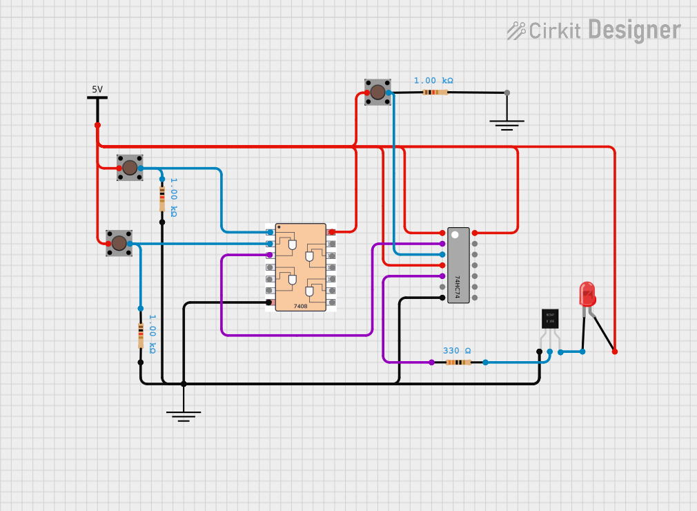 Open Project in Cirkit Designer
Explore Projects Built with SN74HC251
Open Project in Cirkit DesignerOpen Project in Cirkit DesignerOpen Project in Cirkit DesignerOpen Project in Cirkit DesignerCommon Applications
- Data routing in digital systems
- Signal selection in microcontroller-based projects
- Logic control in embedded systems
- Multiplexing in communication systems
- Address decoding in memory systems
Technical Specifications
The SN74HC251 is a high-speed CMOS device with the following key specifications:
| Parameter | Value |
|---|---|
| Supply Voltage (Vcc) | 2V to 6V |
| Input Voltage Range | 0V to Vcc |
| High-Level Input Voltage | 2V (min) at Vcc = 4.5V |
| Low-Level Input Voltage | 0.8V (max) at Vcc = 4.5V |
| High-Level Output Current | -5.2 mA |
| Low-Level Output Current | 5.2 mA |
| Propagation Delay (typical) | 14 ns at Vcc = 5V |
| Operating Temperature Range | -40°C to 85°C |
| Package Types | PDIP, SOIC, TSSOP, SSOP |
Pin Configuration and Descriptions
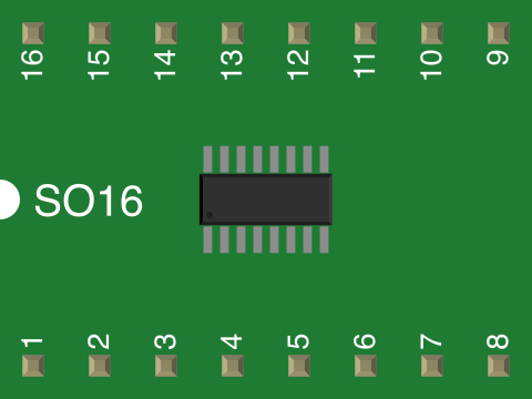
The SN74HC251 has a 16-pin configuration as shown below:
| Pin Number | Pin Name | Description |
|---|---|---|
| 1 | A | Select input A (LSB of select lines) |
| 2 | B | Select input B |
| 3 | C | Select input C (MSB of select lines) |
| 4 | Y | Multiplexer output |
| 5 | W | Complementary output (inverted Y) |
| 6-13 | I0-I7 | Data inputs (8 channels) |
| 14 | G | Enable input (active low) |
| 15 | Vcc | Positive power supply |
| 16 | GND | Ground |
Usage Instructions
How to Use the SN74HC251 in a Circuit
- Power Supply: Connect the Vcc pin to a voltage source within the range of 2V to 6V, and connect the GND pin to the ground of the circuit.
- Input Selection: Use the select pins (A, B, C) to choose one of the eight input channels (I0-I7). The binary combination of A, B, and C determines the selected input.
- For example, if A=0, B=1, and C=0, the multiplexer will select input I2.
- Enable Control: The G pin is an active-low enable input. To enable the multiplexer, set G to a low logic level (0). If G is high (1), the outputs Y and W will be disabled.
- Output: The selected input signal will appear at the Y pin, while its inverted version will appear at the W pin.
Important Considerations
- Ensure that the input voltage levels are within the specified range (0V to Vcc).
- Use pull-up or pull-down resistors on unused input pins to prevent floating inputs.
- Avoid exceeding the maximum current ratings to prevent damage to the device.
- Decouple the power supply with a 0.1 µF capacitor placed close to the Vcc and GND pins to reduce noise.
Example: Connecting SN74HC251 to an Arduino UNO
The SN74HC251 can be easily interfaced with an Arduino UNO for digital signal selection. Below is an example code snippet:
// Arduino example for controlling the SN74HC251 multiplexer
// Connect select pins A, B, C to Arduino pins 2, 3, 4 respectively
// Connect enable pin G to Arduino pin 5 (active low)

const int selectPinA = 2; // Select pin A
const int selectPinB = 3; // Select pin B
const int selectPinC = 4; // Select pin C
const int enablePin = 5;  // Enable pin (active low)

void setup() {
  // Set select and enable pins as outputs
  pinMode(selectPinA, OUTPUT);
  pinMode(selectPinB, OUTPUT);
  pinMode(selectPinC, OUTPUT);
  pinMode(enablePin, OUTPUT);

  // Enable the multiplexer
  digitalWrite(enablePin, LOW);
}

void loop() {
  // Example: Select input I3 (binary 011)
  digitalWrite(selectPinA, HIGH); // A = 1
  digitalWrite(selectPinB, HIGH); // B = 1
  digitalWrite(selectPinC, LOW);  // C = 0

  delay(1000); // Wait for 1 second

  // Example: Select input I5 (binary 101)
  digitalWrite(selectPinA, HIGH); // A = 1
  digitalWrite(selectPinB, LOW);  // B = 0
  digitalWrite(selectPinC, HIGH); // C = 1

  delay(1000); // Wait for 1 second
}
Troubleshooting and FAQs
Common Issues
No Output Signal:
- Ensure the enable pin (G) is set to a low logic level (0).
- Verify that the power supply (Vcc) and ground (GND) connections are correct.
- Check if the select pins (A, B, C) are set to the correct binary combination for the desired input.
Incorrect Output:
- Confirm that the input signals (I0-I7) are within the specified voltage range.
- Ensure there are no floating inputs by using pull-up or pull-down resistors on unused pins.
Noise or Unstable Output:
- Add a decoupling capacitor (0.1 µF) between Vcc and GND to reduce power supply noise.
- Verify that the input signals are clean and free from noise.
FAQs
Q1: Can the SN74HC251 handle analog signals?
A1: No, the SN74HC251 is designed for digital signals only. For analog signals, consider using an analog multiplexer like the CD4051.
Q2: What happens if the enable pin (G) is left floating?
A2: Leaving the enable pin floating can cause unpredictable behavior. Always connect it to a defined logic level (either HIGH or LOW).
Q3: Can I use the SN74HC251 with a 3.3V microcontroller?
A3: Yes, the SN74HC251 operates with supply voltages as low as 2V, making it compatible with 3.3V systems. Ensure that the input and output voltage levels match the microcontroller's logic levels.
This concludes the documentation for the SN74HC251.