
How to Use LT3042+PNP: Examples, Pinouts, and Specs
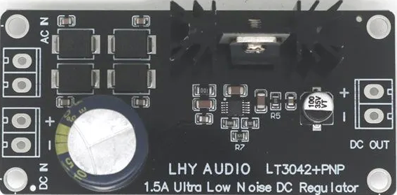
 Design with LT3042+PNP in Cirkit Designer
Introduction
The LT3042 is a high-performance, low noise, low dropout (LDO) linear regulator designed to provide a stable and precise output voltage. It features an innovative architecture with a PNP output stage, enabling high output current capability and excellent transient response. The LT3042 is ideal for applications requiring ultra-low noise and high power supply rejection, such as precision instrumentation, RF systems, and high-speed data converters.
Explore Projects Built with LT3042+PNP
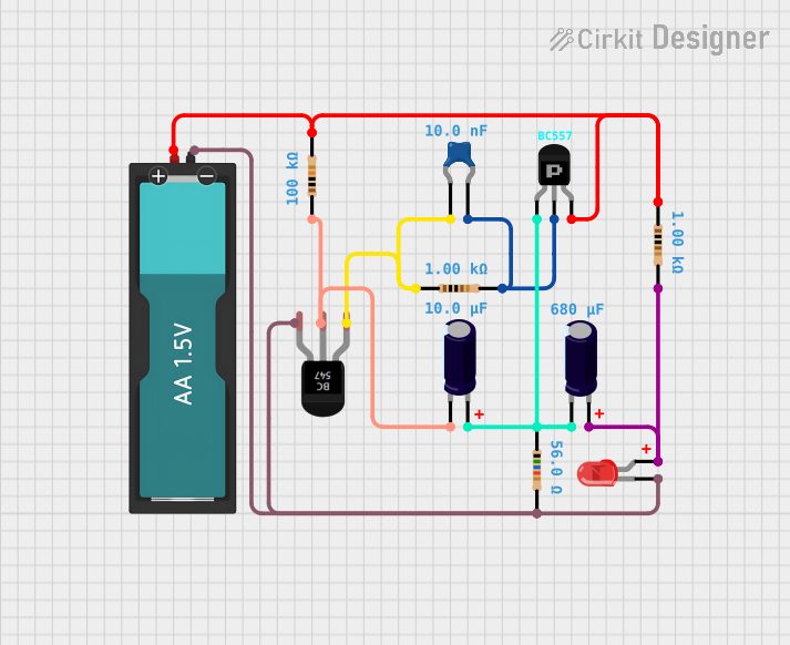 Open Project in Cirkit Designer
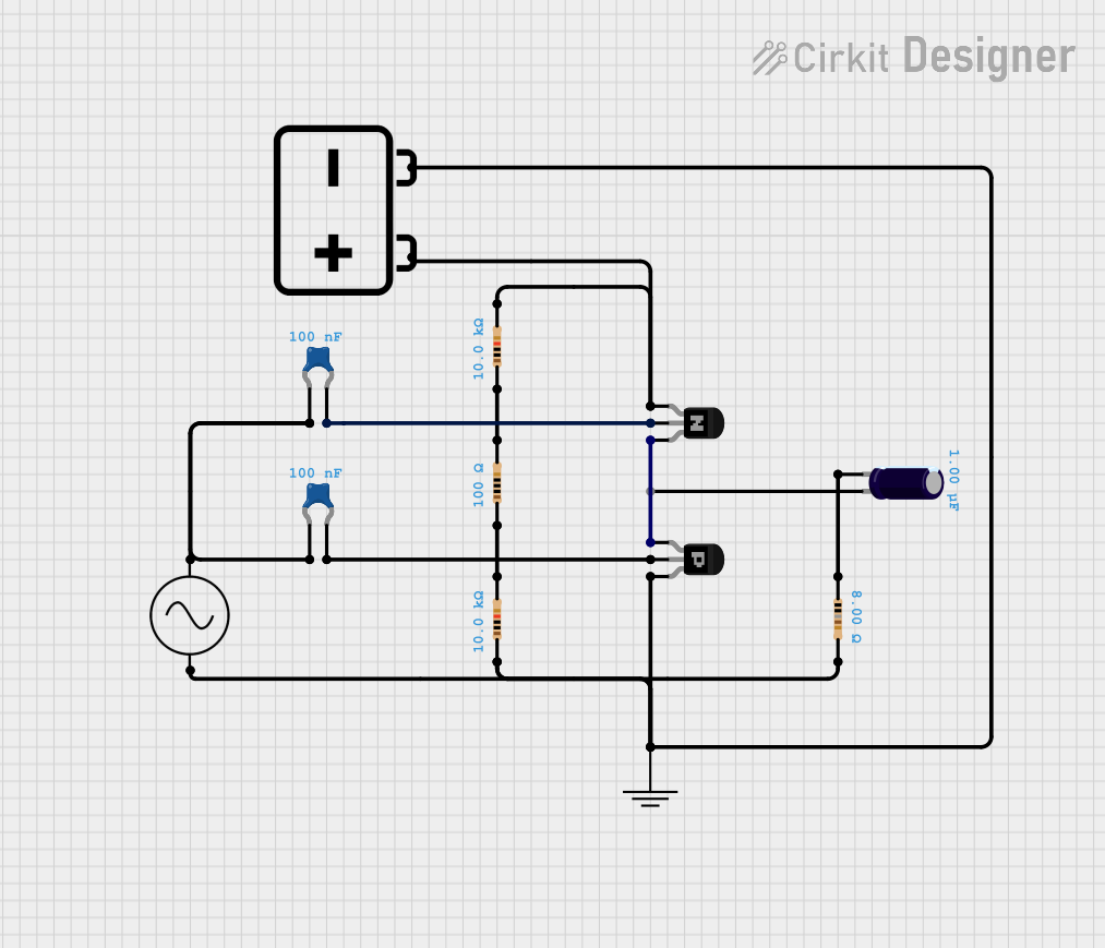 Open Project in Cirkit Designer
 Open Project in Cirkit Designer
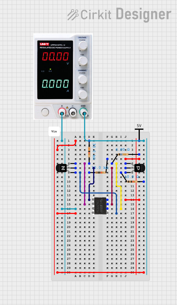 Open Project in Cirkit Designer
Explore Projects Built with LT3042+PNP
Open Project in Cirkit DesignerOpen Project in Cirkit DesignerOpen Project in Cirkit DesignerOpen Project in Cirkit DesignerCommon Applications
- Precision instrumentation and measurement systems
- RF and microwave communication systems
- High-speed data converters (ADCs/DACs)
- Low-noise power supplies for sensitive analog circuits
- Medical devices and test equipment
Technical Specifications
Key Technical Details
| Parameter | Value |
|---|---|
| Input Voltage Range | 2.0V to 20V |
| Output Voltage Range | 0V to 15V (adjustable via external resistors) |
| Maximum Output Current | 200mA |
| Dropout Voltage | 350mV typical at 200mA load |
| Output Noise | 0.8µVRMS (10Hz to 100kHz) |
| Power Supply Rejection | 79dB at 1MHz |
| Operating Temperature Range | -40°C to 125°C |
| Package Options | MSOP-8, DFN-10 |
Pin Configuration and Descriptions
LT3042 Pinout (MSOP-8 Package)
| Pin Number | Pin Name | Description |
|---|---|---|
| 1 | IN | Input voltage supply |
| 2 | GND | Ground |
| 3 | SET | Sets the output voltage via external resistor |
| 4 | OUT | Regulated output voltage |
| 5 | ILIM | Current limit adjustment |
| 6 | BYP | Bypass capacitor connection for noise reduction |
| 7 | NC | No connection (leave floating) |
| 8 | SHDN | Shutdown control (active low) |
LT3042 Pinout (DFN-10 Package)
| Pin Number | Pin Name | Description |
|---|---|---|
| 1 | IN | Input voltage supply |
| 2 | GND | Ground |
| 3 | SET | Sets the output voltage via external resistor |
| 4 | OUT | Regulated output voltage |
| 5 | ILIM | Current limit adjustment |
| 6 | BYP | Bypass capacitor connection for noise reduction |
| 7 | SHDN | Shutdown control (active low) |
| 8 | PG | Power good indicator |
| 9 | NC | No connection (leave floating) |
| 10 | NC | No connection (leave floating) |
Usage Instructions
How to Use the LT3042 in a Circuit
- Input Voltage Supply: Connect the input voltage (2.0V to 20V) to the
INpin. Ensure the input voltage is at least 350mV higher than the desired output voltage. - Output Voltage Setting: Use an external resistor (Rset) between the
SETpin and ground to configure the output voltage. The output voltage is determined by the formula: [ V_{OUT} = I_{SET} \times R_{SET} ] where ( I_{SET} ) is a fixed reference current of 100µA. - Bypass Capacitor: Connect a low ESR capacitor (e.g., 10µF) to the
BYPpin to minimize output noise. - Current Limit Adjustment: Use an external resistor on the
ILIMpin to set the current limit. Refer to the datasheet for resistor values corresponding to desired current limits. - Shutdown Control: To enable the regulator, ensure the
SHDNpin is pulled high. Pulling it low will disable the output. - Output Capacitor: Connect a low ESR capacitor (e.g., 10µF or higher) to the
OUTpin for stability and noise filtering.
Important Considerations
- Use high-quality, low ESR capacitors for the input, output, and bypass connections to ensure optimal performance.
- Keep the traces for the
SETandBYPpins as short as possible to minimize noise pickup. - Ensure proper thermal management, especially when operating at high currents or high input voltages.
Example: Connecting LT3042 to an Arduino UNO
The LT3042 can be used to provide a clean 5V supply to an Arduino UNO. Below is an example circuit and Arduino code to monitor the power good (PG) signal.
Circuit Description
- Connect a 12V DC input to the
INpin of the LT3042. - Set the output voltage to 5V using a 50kΩ resistor on the
SETpin. - Connect the
OUTpin to the Arduino UNO's 5V pin. - Use the
PGpin to monitor the regulator's status.
Arduino Code
// Arduino code to monitor the LT3042 Power Good (PG) signal
const int pgPin = 2; // Connect LT3042 PG pin to Arduino digital pin 2
const int ledPin = 13; // Onboard LED for status indication

void setup() {
  pinMode(pgPin, INPUT); // Set PG pin as input
  pinMode(ledPin, OUTPUT); // Set LED pin as output
  Serial.begin(9600); // Initialize serial communication
}

void loop() {
  int pgStatus = digitalRead(pgPin); // Read the PG pin status

  if (pgStatus == HIGH) {
    digitalWrite(ledPin, HIGH); // Turn on LED if power is good
    Serial.println("Power Good: Regulator output is stable.");
  } else {
    digitalWrite(ledPin, LOW); // Turn off LED if power is not good
    Serial.println("Power Not Good: Check input or load conditions.");
  }

  delay(1000); // Wait for 1 second before checking again
}
Troubleshooting and FAQs
Common Issues
Output Voltage is Incorrect
- Cause: Incorrect resistor value on the
SETpin. - Solution: Verify the resistor value and recalculate using the formula ( V_{OUT} = I_{SET} \times R_{SET} ).
- Cause: Incorrect resistor value on the
Regulator Overheating
- Cause: Excessive power dissipation due to high input-output voltage difference or high load current.
- Solution: Use a heatsink or improve PCB thermal design. Reduce the input voltage if possible.
No Output Voltage
- Cause:
SHDNpin is pulled low or input voltage is too low. - Solution: Ensure the
SHDNpin is pulled high and the input voltage is within the specified range.
- Cause:
High Output Noise
- Cause: Missing or low-quality bypass capacitor on the
BYPpin. - Solution: Add a low ESR capacitor (e.g., 10µF ceramic) to the
BYPpin.
- Cause: Missing or low-quality bypass capacitor on the
FAQs
Q: Can the LT3042 be used for negative voltage regulation?
A: No, the LT3042 is designed for positive voltage regulation only.
Q: What is the maximum output current of the LT3042?
A: The LT3042 can provide up to 200mA of output current.
Q: Is the LT3042 suitable for battery-powered applications?
A: Yes, its low dropout voltage and high efficiency make it suitable for battery-powered systems.
Q: Can I leave the BYP pin unconnected?
A: While the regulator will function without a bypass capacitor, connecting a capacitor to the BYP pin significantly reduces output noise.