How to Use CD4027: Examples, Pinouts, and Specs
Introduction
The CD4027 is a dual D-type flip-flop integrated circuit (IC) designed for use in digital circuits. It is a versatile component that can store and transfer data, making it an essential building block in memory elements, counters, and state machines. Each flip-flop in the CD4027 features independent set (S) and reset (R) inputs, as well as clock (CLK) and data (D) inputs, enabling flexible operation in a wide range of applications.
Explore Projects Built with CD4027
Explore Projects Built with CD4027
Common Applications:
- Data storage and transfer
- Memory elements in digital systems
- Frequency division and counters
- State machines and sequential logic circuits
Technical Specifications
The CD4027 is a CMOS-based IC with the following key specifications:
| Parameter | Value |
|---|---|
| Supply Voltage (VDD) | 3V to 15V |
| Input Voltage Range | 0V to VDD |
| Maximum Clock Frequency | 3 MHz (at 10V supply) |
| Propagation Delay | 200 ns (typical at 10V supply) |
| Power Dissipation | 0.5 mW (typical) |
| Operating Temperature Range | -55°C to +125°C |
| Package Types | DIP-16, SOIC-16 |
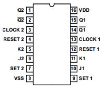
Pin Configuration and Descriptions
The CD4027 is a 16-pin IC with the following pinout:
| Pin Number | Pin Name | Description |
|---|---|---|
| 1 | Q1 | Output of Flip-Flop 1 |
| 2 | Q1̅ | Complementary Output of Flip-Flop 1 |
| 3 | CLK1 | Clock Input for Flip-Flop 1 |
| 4 | R1 | Reset Input for Flip-Flop 1 (Active High) |
| 5 | S1 | Set Input for Flip-Flop 1 (Active High) |
| 6 | D1 | Data Input for Flip-Flop 1 |
| 7 | VSS | Ground (0V) |
| 8 | D2 | Data Input for Flip-Flop 2 |
| 9 | S2 | Set Input for Flip-Flop 2 (Active High) |
| 10 | R2 | Reset Input for Flip-Flop 2 (Active High) |
| 11 | CLK2 | Clock Input for Flip-Flop 2 |
| 12 | Q2̅ | Complementary Output of Flip-Flop 2 |
| 13 | Q2 | Output of Flip-Flop 2 |
| 14 | VDD | Positive Supply Voltage |
| 15 | NC | No Connection |
| 16 | NC | No Connection |
Usage Instructions
How to Use the CD4027 in a Circuit
- Power Supply: Connect the VDD pin (14) to the positive supply voltage (3V to 15V) and the VSS pin (7) to ground.
- Inputs: Provide the desired logic levels to the data (D), clock (CLK), set (S), and reset (R) inputs. Ensure that the input voltage levels are within the specified range (0V to VDD).
- Outputs: The Q and Q̅ pins provide the output states of the flip-flops. These outputs can be connected to other digital components or used to drive LEDs, relays, etc.
- Clock Signal: Apply a clock signal to the CLK pin to trigger the flip-flop. The output state will change based on the data input (D) at the rising edge of the clock signal.
- Set and Reset: Use the S and R pins to force the flip-flop into a set or reset state, regardless of the clock or data inputs.
Important Considerations and Best Practices
- Debounce the Clock Signal: If using a mechanical switch to generate the clock signal, ensure it is debounced to avoid erratic behavior.
- Unused Inputs: Tie unused inputs (D, S, R) to a defined logic level (VDD or VSS) to prevent floating inputs, which can cause unpredictable behavior.
- Bypass Capacitor: Place a 0.1 µF ceramic capacitor close to the VDD and VSS pins to filter out noise and stabilize the power supply.
- Voltage Levels: Ensure that all input signals are within the specified voltage range to avoid damaging the IC.
Example: Connecting the CD4027 to an Arduino UNO
The CD4027 can be interfaced with an Arduino UNO to demonstrate its functionality. Below is an example code to toggle the state of a flip-flop using a clock signal generated by the Arduino.
// Example: Using Arduino to control the CD4027 flip-flop
// Pin connections:
// Arduino Pin 8 -> CLK1 (Pin 3 of CD4027)
// Arduino Pin 9 -> D1 (Pin 6 of CD4027)
// Arduino GND -> VSS (Pin 7 of CD4027)
// Arduino 5V -> VDD (Pin 14 of CD4027)

const int clockPin = 8; // Clock signal pin
const int dataPin = 9;  // Data input pin

void setup() {
  pinMode(clockPin, OUTPUT); // Set clock pin as output
  pinMode(dataPin, OUTPUT);  // Set data pin as output
}

void loop() {
  digitalWrite(dataPin, HIGH); // Set data input to HIGH
  digitalWrite(clockPin, HIGH); // Generate a rising edge on the clock
  delay(10);                   // Short delay
  digitalWrite(clockPin, LOW); // Generate a falling edge on the clock
  delay(1000);                 // Wait for 1 second

  digitalWrite(dataPin, LOW);  // Set data input to LOW
  digitalWrite(clockPin, HIGH); // Generate another rising edge
  delay(10);                   // Short delay
  digitalWrite(clockPin, LOW); // Generate a falling edge
  delay(1000);                 // Wait for 1 second
}
Troubleshooting and FAQs
Common Issues and Solutions
No Output on Q or Q̅ Pins:
- Ensure that the IC is powered correctly (check VDD and VSS connections).
- Verify that the clock signal is being applied to the CLK pin.
- Check that the data input (D) is not floating and is set to a defined logic level.
Erratic Behavior:
- Debounce the clock signal if using a mechanical switch.
- Add a bypass capacitor (0.1 µF) near the power supply pins to reduce noise.
Flip-Flop Not Responding to Clock Signal:
- Confirm that the set (S) and reset (R) inputs are not active (both should be LOW for normal operation).
- Check the clock signal's voltage levels and ensure they meet the IC's requirements.
FAQs
Q1: Can the CD4027 operate at 5V?
Yes, the CD4027 can operate at a supply voltage of 5V. Ensure that all input signals are within the range of 0V to 5V.
Q2: What happens if both S and R inputs are HIGH?
If both the set (S) and reset (R) inputs are HIGH simultaneously, the behavior is undefined, and the outputs may enter an invalid state. Avoid this condition in your circuit design.
Q3: Can the CD4027 be used for frequency division?
Yes, the CD4027 can be configured as a toggle flip-flop to divide the frequency of a clock signal by 2. Connect the Q output to the D input and apply the clock signal to the CLK pin.
Q4: Is the CD4027 compatible with TTL logic levels?
The CD4027 is a CMOS IC and may not be directly compatible with TTL logic levels. Use a level shifter or ensure that the input voltage levels meet the IC's requirements.