
How to Use ZVS Capacitor Charging: Examples, Pinouts, and Specs
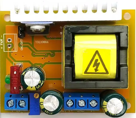
 Design with ZVS Capacitor Charging in Cirkit Designer
Introduction
The ZVS (Zero Voltage Switching) Capacitor Charging circuit, manufactured by Texas Instruments (TI) with part ID ZVS, is a highly efficient circuit configuration designed to charge capacitors while minimizing voltage spikes. This component is particularly useful in applications requiring high voltage and fast charging times, such as laser systems, pulsed power supplies, and high-energy physics experiments. By employing zero voltage switching, the circuit reduces switching losses and electromagnetic interference (EMI), ensuring reliable and efficient operation.
Explore Projects Built with ZVS Capacitor Charging
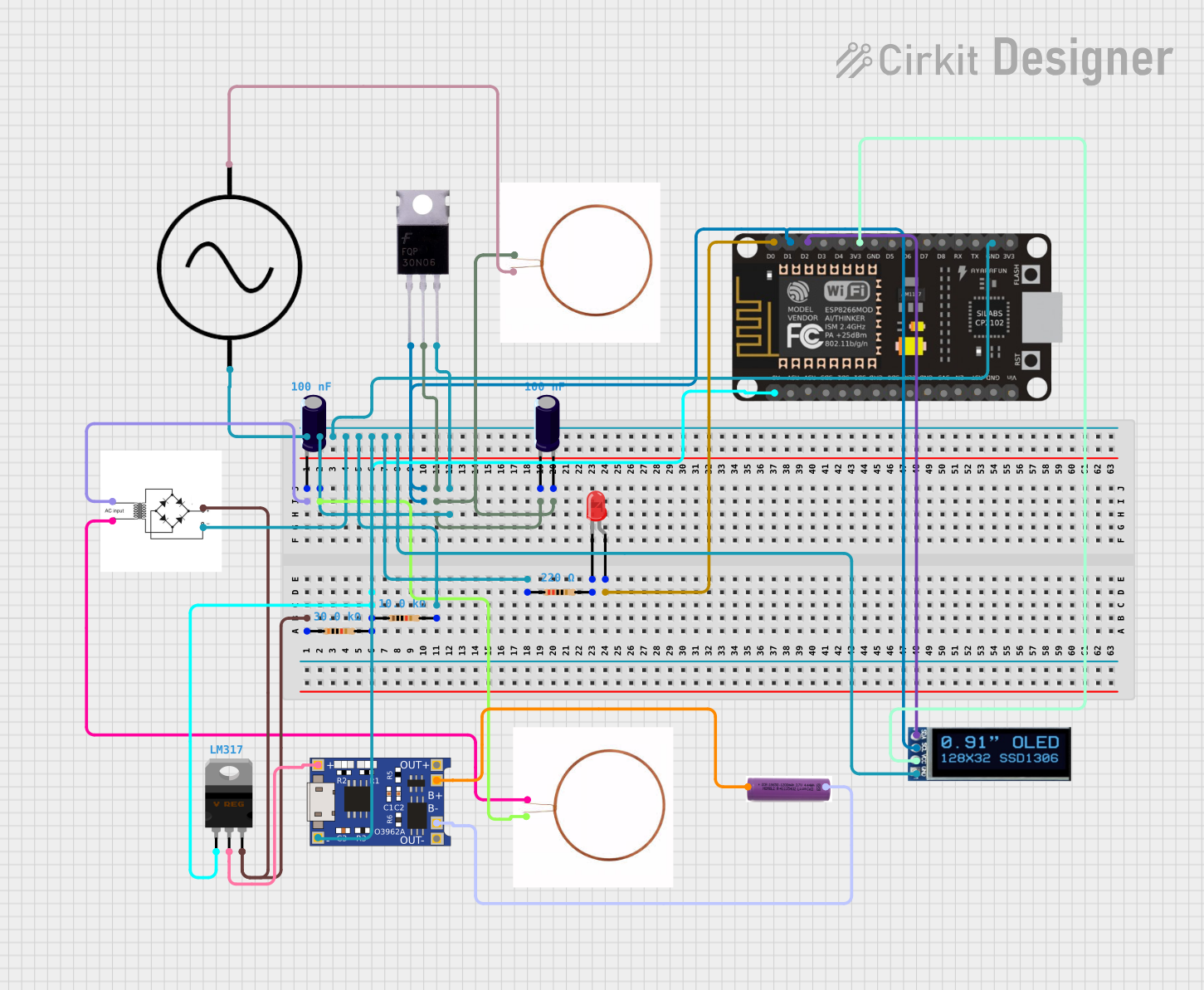 Open Project in Cirkit Designer
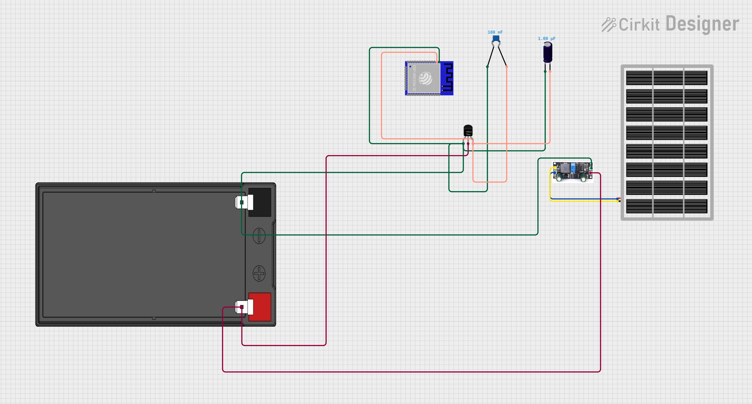 Open Project in Cirkit Designer
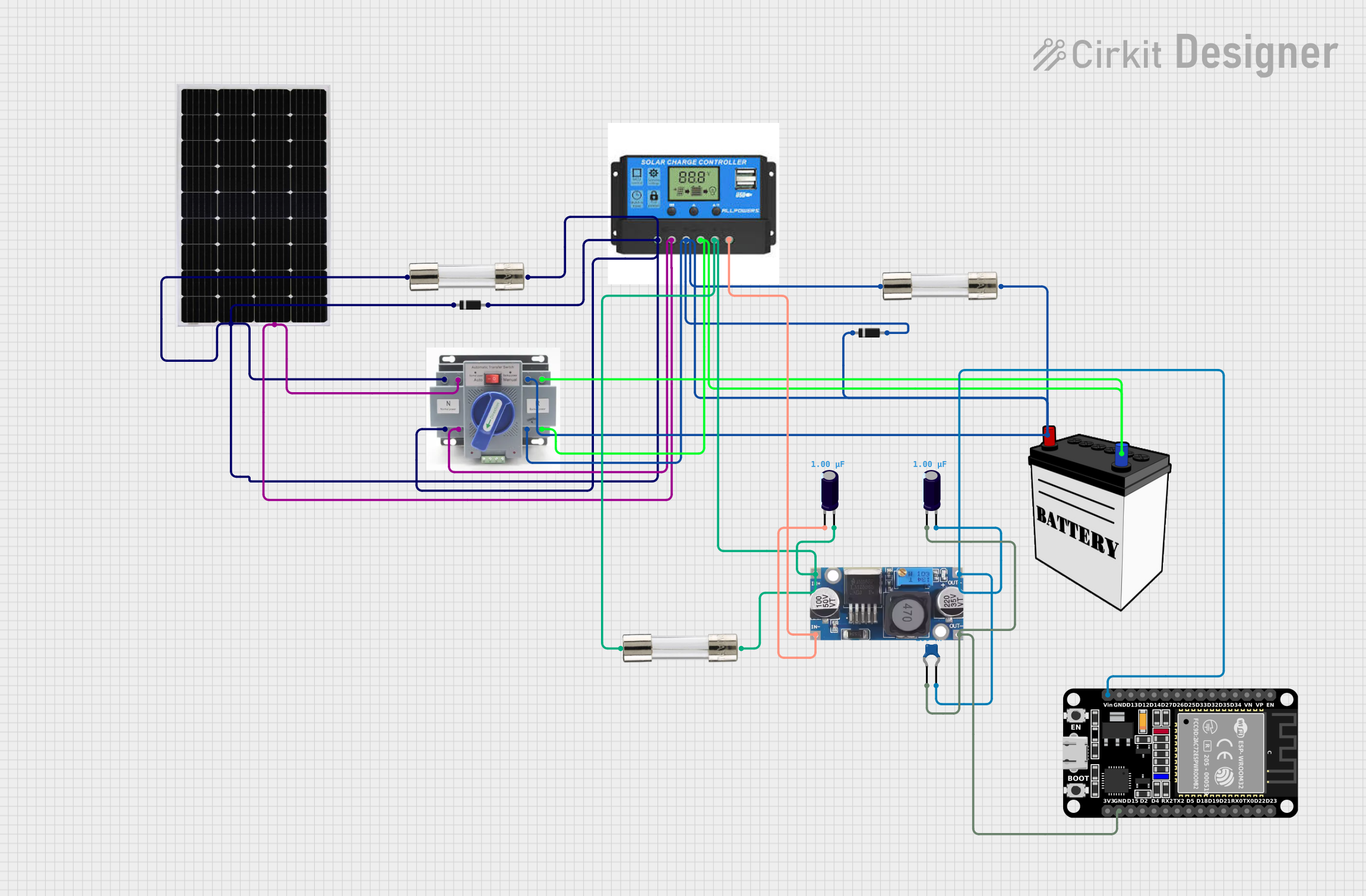 Open Project in Cirkit Designer
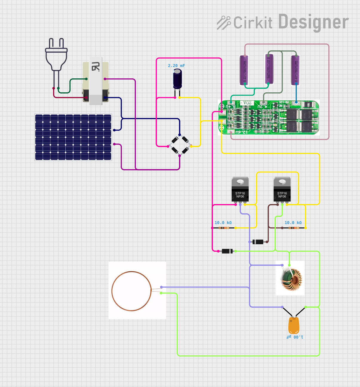 Open Project in Cirkit Designer
Explore Projects Built with ZVS Capacitor Charging
Open Project in Cirkit DesignerOpen Project in Cirkit DesignerOpen Project in Cirkit DesignerOpen Project in Cirkit DesignerCommon Applications
- Laser power supplies
- High-voltage capacitor banks
- Pulsed power systems
- Medical imaging equipment
- Industrial power systems
Technical Specifications
Key Technical Details
| Parameter | Value |
|---|---|
| Input Voltage Range | 12V to 48V |
| Output Voltage Range | Up to 500V (depending on design) |
| Switching Frequency | 20 kHz to 100 kHz |
| Efficiency | Up to 95% |
| Maximum Output Current | 10A (depending on configuration) |
| Operating Temperature Range | -40°C to +85°C |
Pin Configuration and Descriptions
The ZVS Capacitor Charging circuit typically consists of several key components, including MOSFETs, diodes, and inductors. Below is a general description of the pin configuration for a typical ZVS module:
| Pin Number | Pin Name | Description |
|---|---|---|
| 1 | VIN+ | Positive input voltage terminal. Connect to the DC power supply. |
| 2 | VIN- | Negative input voltage terminal. Connect to the ground of the power supply. |
| 3 | HV OUT+ | High-voltage positive output terminal. Connect to the capacitor to be charged. |
| 4 | HV OUT- | High-voltage negative output terminal. Connect to the capacitor ground. |
| 5 | ENABLE | Enable pin. Apply a logic HIGH signal to activate the circuit. |
| 6 | GND | Ground pin for control signals. |
Usage Instructions
How to Use the ZVS Capacitor Charging Circuit
- Power Supply Connection: Connect the input voltage (VIN+ and VIN-) to a DC power supply within the specified input voltage range (12V to 48V). Ensure the power supply can provide sufficient current for the application.
- Capacitor Connection: Connect the capacitor to be charged across the HV OUT+ and HV OUT- terminals. Ensure the capacitor's voltage rating exceeds the maximum output voltage of the circuit.
- Enable the Circuit: Apply a logic HIGH signal to the ENABLE pin to activate the circuit. The ZVS circuit will begin charging the capacitor.
- Monitor Output Voltage: Use a voltmeter or other monitoring device to ensure the capacitor is charged to the desired voltage level.
Important Considerations and Best Practices
- Heat Dissipation: Ensure adequate cooling for the MOSFETs and other components to prevent overheating. Use heat sinks or active cooling if necessary.
- Safety Precautions: High voltages can be dangerous. Always discharge capacitors before handling the circuit and use proper insulation.
- Component Ratings: Verify that all components, including capacitors and diodes, are rated for the desired voltage and current levels.
- Switching Frequency: Adjust the switching frequency to optimize efficiency and minimize EMI. This can typically be done by modifying the circuit's control parameters.
Example Code for Arduino UNO
The ZVS Capacitor Charging circuit can be controlled using an Arduino UNO. Below is an example code snippet to enable and disable the circuit using a digital pin:
// Define the pin connected to the ENABLE pin of the ZVS circuit
const int enablePin = 7;

void setup() {
  // Set the enablePin as an output
  pinMode(enablePin, OUTPUT);

  // Start with the ZVS circuit disabled
  digitalWrite(enablePin, LOW);
}

void loop() {
  // Enable the ZVS circuit for 5 seconds
  digitalWrite(enablePin, HIGH); // Activate the circuit
  delay(5000);                   // Wait for 5 seconds

  // Disable the ZVS circuit
  digitalWrite(enablePin, LOW);  // Deactivate the circuit
  delay(5000);                   // Wait for 5 seconds
}
Note: Ensure the Arduino's ground (GND) is connected to the ZVS circuit's ground (GND) for proper operation.
Troubleshooting and FAQs
Common Issues and Solutions
Issue: The capacitor is not charging.
- Solution: Verify the input voltage and ensure it is within the specified range. Check the ENABLE pin signal and ensure it is set to HIGH. Inspect all connections for loose or incorrect wiring.
Issue: The circuit overheats during operation.
- Solution: Ensure proper heat dissipation for the MOSFETs and other components. Use heat sinks or active cooling if necessary. Reduce the input voltage or output current if possible.
Issue: High levels of electromagnetic interference (EMI).
- Solution: Adjust the switching frequency to minimize EMI. Use shielded cables and proper grounding techniques.
Issue: The output voltage exceeds the capacitor's rating.
- Solution: Use a capacitor with a higher voltage rating or adjust the circuit's output voltage limit.
FAQs
Q: Can the ZVS circuit charge multiple capacitors simultaneously?
A: Yes, but ensure the total capacitance and voltage ratings are within the circuit's specifications. Use proper wiring to distribute the charge evenly.Q: What is the typical efficiency of the ZVS circuit?
A: The ZVS circuit can achieve efficiencies of up to 95%, depending on the input voltage, output voltage, and load conditions.Q: Is it safe to use the ZVS circuit for medical applications?
A: Yes, but ensure compliance with all relevant safety and regulatory standards for medical devices.Q: Can the circuit operate at higher input voltages?
A: The input voltage range is limited to 12V to 48V. Exceeding this range may damage the circuit.
By following this documentation, users can effectively utilize the ZVS Capacitor Charging circuit for a wide range of high-voltage applications.