Cirkit Designer Logo
Cirkit Designer
Your all-in-one circuit design IDE
Home / 
Component Documentation

How to Use 4013: Examples, Pinouts, and Specs

Image of 4013
Cirkit Designer LogoDesign with 4013 in Cirkit Designer

Introduction

The CD4013 is a CMOS Dual D-Type Flip-Flop integrated circuit. Each flip-flop has independent data, set, reset, and clock inputs and Q and Q\ outputs. This component is widely used in digital electronics for storing and transferring data based on clock signals. Common applications include:

  • Signal buffering
  • Data storage
  • Frequency division
  • Shift registers
  • Counters

Explore Projects Built with 4013

Use Cirkit Designer to design, explore, and prototype these projects online. Some projects support real-time simulation. Click "Open Project" to start designing instantly!
Digital Logic State Indicator with Flip-Flops and Logic Gates
Image of 2-bit Gray Code Counter: A project utilizing 4013 in a practical application
This circuit is a digital logic system that uses a DIP switch to provide input to a network of flip-flops and logic gates, which process the input signals. The output of this processing is likely indicated by LEDs, which are connected through resistors to limit current. The circuit functions autonomously without a microcontroller, relying on the inherent properties of the digital components to perform its logic operations.
Cirkit Designer LogoOpen Project in Cirkit Designer
NFC-Enabled Access Control System with Time Logging
Image of doorlock: A project utilizing 4013 in a practical application
This circuit is designed for access control with time tracking capabilities. It features an NFC/RFID reader for authentication, an RTC module (DS3231) for real-time clock functionality, and an OLED display for user interaction. A 12V relay controls a magnetic lock, which is activated upon successful NFC/RFID authentication, and a button switch is likely used for manual operation or input. The T8_S3 microcontroller serves as the central processing unit, interfacing with the NFC/RFID reader, RTC, OLED, and relay to manage the access control logic.
Cirkit Designer LogoOpen Project in Cirkit Designer
Arduino Nano 33 BLE Battery-Powered Display Interface
Image of senior design 1: A project utilizing 4013 in a practical application
This circuit features a Nano 33 BLE microcontroller interfaced with a TM1637 4-digit 7-segment display for information output, powered by a 3.7V battery managed by a TP4056 charging module. The microcontroller communicates with the display to present data, while the TP4056 ensures the battery is charged safely and provides power to the system.
Cirkit Designer LogoOpen Project in Cirkit Designer
Arduino UNO Controlled Relay with DS3231 RTC
Image of Hooter connections: A project utilizing 4013 in a practical application
This circuit features an Arduino UNO microcontroller connected to a DS3231 Real Time Clock (RTC) module and a 12V single-channel relay. The Arduino provides power to both the RTC and the relay, and it communicates with the RTC via I2C using the SDA and SCL lines connected to A4 and A5 respectively. The relay is controlled by the Arduino through a digital output on pin D13, allowing the Arduino to switch external loads on and off based on time events managed by the RTC.
Cirkit Designer LogoOpen Project in Cirkit Designer

Explore Projects Built with 4013

Use Cirkit Designer to design, explore, and prototype these projects online. Some projects support real-time simulation. Click "Open Project" to start designing instantly!
Image of 2-bit Gray Code Counter: A project utilizing 4013 in a practical application
Digital Logic State Indicator with Flip-Flops and Logic Gates
This circuit is a digital logic system that uses a DIP switch to provide input to a network of flip-flops and logic gates, which process the input signals. The output of this processing is likely indicated by LEDs, which are connected through resistors to limit current. The circuit functions autonomously without a microcontroller, relying on the inherent properties of the digital components to perform its logic operations.
Cirkit Designer LogoOpen Project in Cirkit Designer
Image of doorlock: A project utilizing 4013 in a practical application
NFC-Enabled Access Control System with Time Logging
This circuit is designed for access control with time tracking capabilities. It features an NFC/RFID reader for authentication, an RTC module (DS3231) for real-time clock functionality, and an OLED display for user interaction. A 12V relay controls a magnetic lock, which is activated upon successful NFC/RFID authentication, and a button switch is likely used for manual operation or input. The T8_S3 microcontroller serves as the central processing unit, interfacing with the NFC/RFID reader, RTC, OLED, and relay to manage the access control logic.
Cirkit Designer LogoOpen Project in Cirkit Designer
Image of senior design 1: A project utilizing 4013 in a practical application
Arduino Nano 33 BLE Battery-Powered Display Interface
This circuit features a Nano 33 BLE microcontroller interfaced with a TM1637 4-digit 7-segment display for information output, powered by a 3.7V battery managed by a TP4056 charging module. The microcontroller communicates with the display to present data, while the TP4056 ensures the battery is charged safely and provides power to the system.
Cirkit Designer LogoOpen Project in Cirkit Designer
Image of Hooter connections: A project utilizing 4013 in a practical application
Arduino UNO Controlled Relay with DS3231 RTC
This circuit features an Arduino UNO microcontroller connected to a DS3231 Real Time Clock (RTC) module and a 12V single-channel relay. The Arduino provides power to both the RTC and the relay, and it communicates with the RTC via I2C using the SDA and SCL lines connected to A4 and A5 respectively. The relay is controlled by the Arduino through a digital output on pin D13, allowing the Arduino to switch external loads on and off based on time events managed by the RTC.
Cirkit Designer LogoOpen Project in Cirkit Designer

Technical Specifications

General Characteristics

  • Supply Voltage (Vdd): 3V to 15V
  • Input Voltage (Vin): -0.5V to Vdd + 0.5V
  • Operating Temperature: -55°C to +125°C
  • Output Current: ±6.8 mA
  • Propagation Delay Time: 50 ns (typical at Vdd = 10V)
  • Power Dissipation: 500 mW

Pin Configuration and Descriptions

Pin Number Name Description
1 Q1 Output of flip-flop 1
2 Q1\ Complementary output of flip-flop 1
3 CLK1 Clock input of flip-flop 1
4 RST1 Reset input of flip-flop 1 (active HIGH)
5 D1 Data input of flip-flop 1
6 SET1 Set input of flip-flop 1 (active HIGH)
7 GND Ground (0V)
8 SET2 Set input of flip-flop 2 (active HIGH)
9 D2 Data input of flip-flop 2
10 RST2 Reset input of flip-flop 2 (active HIGH)
11 CLK2 Clock input of flip-flop 2
12 Q2\ Complementary output of flip-flop 2
13 Q2 Output of flip-flop 2
14 Vdd Positive supply voltage

Usage Instructions

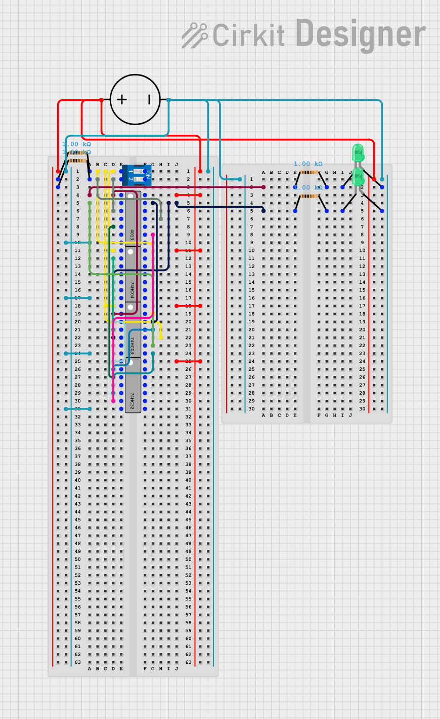
Basic Circuit Connection

To use the CD4013 in a circuit:

  1. Connect Vdd (pin 14) to your power supply (3V to 15V).
  2. Connect GND (pin 7) to the ground of your power supply.
  3. Apply the data signal to the D input (pin 5 for flip-flop 1 or pin 9 for flip-flop 2).
  4. Apply the clock signal to the CLK input (pin 3 for flip-flop 1 or pin 11 for flip-flop 2).
  5. The Q and Q\ outputs (pins 1 and 2 for flip-flop 1, pins 13 and 12 for flip-flop 2) will reflect the stored data based on the clock signal.

Best Practices

  • Use a decoupling capacitor (0.1 µF) close to the Vdd pin to filter out noise.
  • Avoid floating inputs by connecting unused set and reset pins to ground.
  • Ensure that the clock signal has clean rising and falling edges to prevent glitches.

Example with Arduino UNO

// Example code to control a CD4013 flip-flop with an Arduino UNO

const int clockPin = 2; // Connect to CLK1 (pin 3 of CD4013)
const int dataPin = 3;  // Connect to D1 (pin 5 of CD4013)
const int resetPin = 4; // Connect to RST1 (pin 4 of CD4013)

void setup() {
  pinMode(clockPin, OUTPUT);
  pinMode(dataPin, OUTPUT);
  pinMode(resetPin, OUTPUT);
  
  // Reset the flip-flop at the start
  digitalWrite(resetPin, HIGH);
  delay(10);
  digitalWrite(resetPin, LOW);
}

void loop() {
  // Set data to HIGH
  digitalWrite(dataPin, HIGH);
  // Toggle the clock to store the data
  digitalWrite(clockPin, HIGH);
  delay(10);
  digitalWrite(clockPin, LOW);
  
  // Set data to LOW
  digitalWrite(dataPin, LOW);
  // Toggle the clock to store the new data
  digitalWrite(clockPin, HIGH);
  delay(10);
  digitalWrite(clockPin, LOW);
  
  // Add a delay between cycles
  delay(1000);
}

Troubleshooting and FAQs

Common Issues

  • Unstable Outputs: Ensure that all unused inputs are tied to either Vdd or GND to prevent floating inputs.
  • No Output Change on Clock Pulse: Check if the set or reset pins are inadvertently activated or if the data input is not changing.
  • Glitches on Output: Verify that the clock signal is clean and without noise. Use a pull-up or pull-down resistor on the clock line if necessary.

FAQs

Q: Can I use the CD4013 at 5V? A: Yes, the CD4013 can operate at 5V, which is within its supply voltage range.

Q: What is the maximum frequency the CD4013 can handle? A: The maximum frequency depends on the supply voltage. At 10V, the typical propagation delay is 50 ns, which corresponds to a maximum frequency of about 10 MHz.

Q: How do I reset the flip-flop? A: Apply a HIGH signal to the reset pin (RST1 or RST2). The output Q will go LOW, and Q\ will go HIGH.

Q: Can I chain multiple CD4013s together? A: Yes, you can connect the output of one flip-flop to the data input of another to create shift registers or counters.

This documentation provides a comprehensive guide to using the CD4013 Dual D-type Flip-Flop. For further information, consult the manufacturer's datasheet.