How to Use ADS1220: Examples, Pinouts, and Specs
Introduction
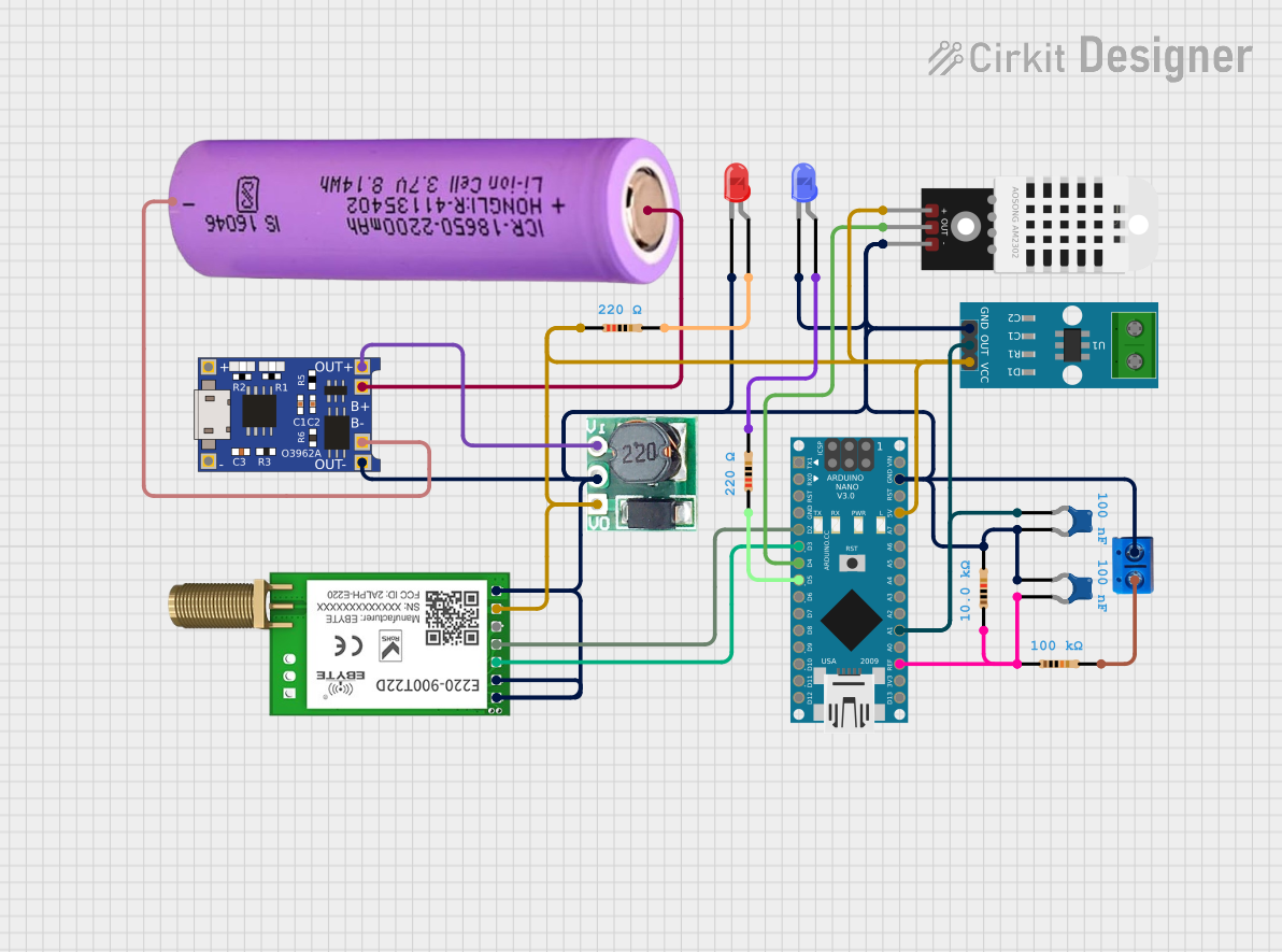
The ADS1220 is a 24-bit analog-to-digital converter (ADC) designed for precision measurement applications. It features a low-noise, low-drift architecture, and includes programmable gain amplifiers (PGAs), making it ideal for interfacing with sensors and performing high-accuracy data acquisition. The ADS1220 is commonly used in industrial, medical, and scientific applications where precise and reliable measurements are critical.
Explore Projects Built with ADS1220
Explore Projects Built with ADS1220
Common Applications
- Temperature measurement using thermocouples or RTDs
- Pressure sensors and strain gauges
- Industrial process control
- Medical instrumentation
- Portable measurement devices
Technical Specifications
The ADS1220 offers a range of features that make it a versatile and high-performance ADC. Below are its key technical specifications:
| Parameter | Value |
|---|---|
| Resolution | 24-bit |
| Input Channels | 4 single-ended or 2 differential |
| Programmable Gain Amplifier | 1x to 128x |
| Data Rates | 20 SPS to 2000 SPS |
| Supply Voltage | 2.3 V to 5.5 V |
| Input Voltage Range | ±VREF / Gain |
| Reference Voltage | Internal (2.048 V) or external |
| Interface | SPI |
| Operating Temperature Range | -40°C to +125°C |
| Package | 16-pin TSSOP |
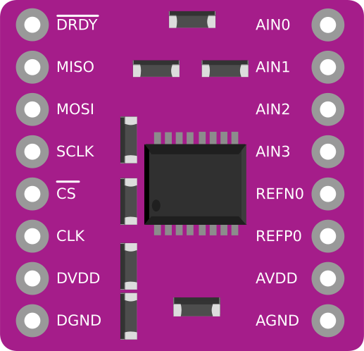
Pin Configuration and Descriptions
The ADS1220 is available in a 16-pin TSSOP package. Below is the pinout and description:
| Pin | Name | Type | Description |
|---|---|---|---|
| 1 | AVDD | Power | Analog power supply (2.3 V to 5.5 V). |
| 2 | DVDD | Power | Digital power supply (1.8 V to 3.6 V). |
| 3 | GND | Ground | Ground reference for both analog and digital circuits. |
| 4 | AIN0 | Analog In | Analog input channel 0. |
| 5 | AIN1 | Analog In | Analog input channel 1. |
| 6 | AIN2 | Analog In | Analog input channel 2. |
| 7 | AIN3 | Analog In | Analog input channel 3. |
| 8 | REFP | Analog In | Positive reference input. |
| 9 | REFN | Analog In | Negative reference input. |
| 10 | DRDY/DOUT | Digital I/O | Data ready output and SPI data output. |
| 11 | SCLK | Digital In | SPI clock input. |
| 12 | CS | Digital In | Chip select input (active low). |
| 13 | DIN | Digital In | SPI data input. |
| 14 | START | Digital In | Start conversion input (active high). |
| 15 | RESET | Digital In | Reset input (active low). |
| 16 | NC | - | No connection. |
Usage Instructions
The ADS1220 is typically used in precision measurement circuits. Below are the steps and considerations for using the ADS1220:
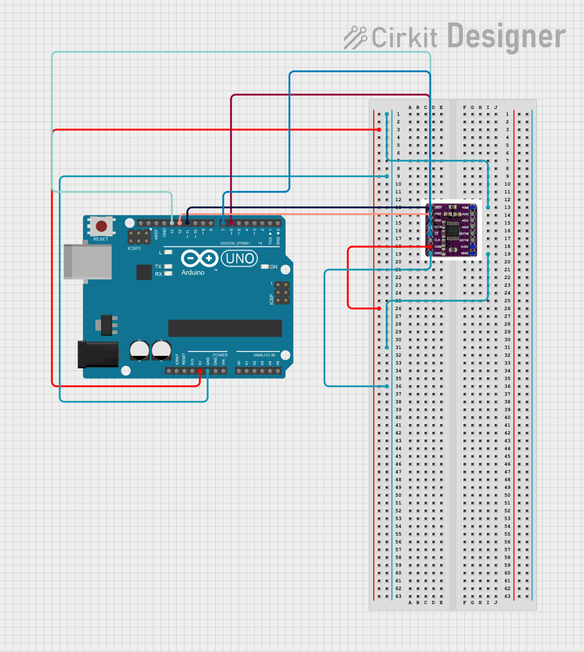
Connecting the ADS1220
- Power Supply: Connect AVDD and DVDD to appropriate power sources (e.g., 3.3 V or 5 V for AVDD, and 3.3 V for DVDD). Connect GND to the system ground.
- Analog Inputs: Connect the sensor or signal source to the AINx pins. For differential measurements, use pairs of AIN pins (e.g., AIN0 and AIN1).
- Reference Voltage: Use the internal reference or connect an external reference voltage to REFP and REFN.
- SPI Interface: Connect the SPI pins (SCLK, DIN, DOUT, and CS) to a microcontroller or processor.
Configuring the ADS1220
- Use the SPI interface to configure the ADS1220's registers. Key settings include:
- Input Multiplexer: Select the input channel or differential pair.
- Gain: Set the PGA gain (1x to 128x).
- Data Rate: Choose the desired data rate (20 SPS to 2000 SPS).
- Reference Source: Select internal or external reference.
Example: Using ADS1220 with Arduino UNO
Below is an example of how to interface the ADS1220 with an Arduino UNO using SPI:
#include <SPI.h>

// Pin definitions
#define CS_PIN 10  // Chip select pin
#define DRDY_PIN 9 // Data ready pin

void setup() {
  // Initialize SPI
  SPI.begin();
  pinMode(CS_PIN, OUTPUT);
  pinMode(DRDY_PIN, INPUT);
  digitalWrite(CS_PIN, HIGH); // Set CS high to deselect ADS1220

  // Configure ADS1220
  configureADS1220();
}

void loop() {
  // Wait for data ready signal
  if (digitalRead(DRDY_PIN) == LOW) {
    long adcValue = readADC();
    Serial.println(adcValue); // Print ADC value
  }
}

void configureADS1220() {
  digitalWrite(CS_PIN, LOW); // Select ADS1220
  SPI.transfer(0x40);        // Write to configuration register 0
  SPI.transfer(0x01);        // Set PGA gain to 1x, select AIN0-AIN1
  SPI.transfer(0x04);        // Set data rate to 20 SPS
  SPI.transfer(0x10);        // Enable internal reference
  digitalWrite(CS_PIN, HIGH); // Deselect ADS1220
}

long readADC() {
  digitalWrite(CS_PIN, LOW); // Select ADS1220
  SPI.transfer(0x10);        // Send read data command
  long result = 0;
  result |= SPI.transfer(0x00) << 16; // Read MSB
  result |= SPI.transfer(0x00) << 8;  // Read middle byte
  result |= SPI.transfer(0x00);       // Read LSB
  digitalWrite(CS_PIN, HIGH); // Deselect ADS1220
  return result;
}
Best Practices
- Use decoupling capacitors (e.g., 0.1 µF and 10 µF) near the power supply pins to reduce noise.
- Ensure proper grounding to minimize interference.
- Use shielded cables for long sensor connections to reduce EMI.
Troubleshooting and FAQs
Common Issues
No Data Output:
- Ensure the SPI connections are correct.
- Verify that the CS pin is being toggled correctly.
- Check the power supply and reference voltage connections.
Incorrect Measurements:
- Verify the input signal is within the ADC's input range.
- Check the PGA gain and input multiplexer settings.
- Ensure the reference voltage is stable and accurate.
High Noise in Readings:
- Use a lower data rate to reduce noise.
- Add filtering capacitors to the input signal.
FAQs
Q: Can I use the ADS1220 with a 5 V microcontroller?
A: Yes, the ADS1220 supports a supply voltage of up to 5.5 V. Ensure the SPI logic levels are compatible with the microcontroller.
Q: How do I measure a thermocouple with the ADS1220?
A: Connect the thermocouple to a differential input pair (e.g., AIN0 and AIN1). Use the internal reference and configure the PGA for the appropriate gain.
Q: What is the maximum sampling rate of the ADS1220?
A: The maximum data rate is 2000 samples per second (SPS).