
How to Use AT25FS010: Examples, Pinouts, and Specs
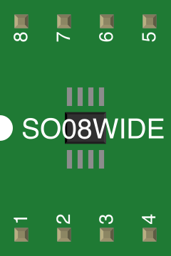
 Design with AT25FS010 in Cirkit Designer
Introduction
The AT25FS010 is a 1 Mbit (128 K x 8) serial Flash memory device designed for non-volatile data storage. It operates on a single power supply and utilizes the SPI (Serial Peripheral Interface) protocol for high-speed data transfer. This component is ideal for applications requiring reliable storage of firmware, configuration data, or other critical information in embedded systems.
Explore Projects Built with AT25FS010
 Open Project in Cirkit Designer
 Open Project in Cirkit Designer
 Open Project in Cirkit Designer
 Open Project in Cirkit Designer
Explore Projects Built with AT25FS010
Open Project in Cirkit DesignerOpen Project in Cirkit DesignerOpen Project in Cirkit DesignerOpen Project in Cirkit DesignerCommon Applications
- Firmware storage for microcontrollers
- Configuration data storage in IoT devices
- Data logging in industrial systems
- Boot code storage for embedded systems
- Non-volatile memory for consumer electronics
Technical Specifications
Key Technical Details
| Parameter | Value |
|---|---|
| Memory Size | 1 Mbit (128 K x 8) |
| Interface | SPI (Serial Peripheral Interface) |
| Operating Voltage | 2.7V to 3.6V |
| Maximum Clock Frequency | 85 MHz |
| Write/Erase Endurance | 100,000 cycles (typical) |
| Data Retention | 20 years (typical) |
| Operating Temperature | -40°C to +85°C |
| Package Options | 8-lead SOIC, 8-lead TSSOP |
Pin Configuration and Descriptions
The AT25FS010 is typically available in an 8-pin package. Below is the pin configuration and description:
| Pin No. | Pin Name | Description |
|---|---|---|
| 1 | CS | Chip Select: Activates the device when pulled low. |
| 2 | SO | Serial Output: Data output pin for SPI communication. |
| 3 | WP | Write Protect: Protects certain memory regions from being written. |
| 4 | GND | Ground: Connect to system ground. |
| 5 | SI | Serial Input: Data input pin for SPI communication. |
| 6 | SCK | Serial Clock: Clock signal for SPI communication. |
| 7 | HOLD | Hold: Pauses communication without resetting the SPI bus. |
| 8 | VCC | Power Supply: Connect to a 2.7V to 3.6V power source. |
Usage Instructions
How to Use the AT25FS010 in a Circuit
- Power Supply: Connect the VCC pin to a 2.7V to 3.6V power source and the GND pin to ground.
- SPI Connections: Connect the SCK, SI, and SO pins to the corresponding SPI pins on your microcontroller. Use the CS pin to enable or disable the device.
- Write Protection: If write protection is required, connect the WP pin to ground. Otherwise, connect it to VCC.
- Hold Function: If the hold function is not used, connect the HOLD pin to VCC.
- Pull-Up Resistors: Use pull-up resistors on the CS, WP, and HOLD pins if necessary to ensure proper operation.
Important Considerations
- Ensure the SPI clock frequency does not exceed 85 MHz.
- Use decoupling capacitors (e.g., 0.1 µF) near the VCC pin to stabilize the power supply.
- Avoid exceeding the write/erase endurance limit to maintain data integrity.
- Follow the timing requirements specified in the datasheet for reliable operation.
Example Code for Arduino UNO
Below is an example of how to interface the AT25FS010 with an Arduino UNO using the SPI library:
#include <SPI.h>

// Define SPI pins for the AT25FS010
const int CS_PIN = 10; // Chip Select pin connected to Arduino pin 10

void setup() {
  // Initialize Serial Monitor for debugging
  Serial.begin(9600);

  // Set up SPI and Chip Select pin
  pinMode(CS_PIN, OUTPUT);
  digitalWrite(CS_PIN, HIGH); // Ensure the chip is deselected
  SPI.begin(); // Initialize SPI communication

  // Test communication with the AT25FS010
  Serial.println("Initializing AT25FS010...");
  readDeviceID();
}

void loop() {
  // Main loop does nothing in this example
}

// Function to read the device ID of the AT25FS010
void readDeviceID() {
  digitalWrite(CS_PIN, LOW); // Select the chip
  SPI.transfer(0x9F); // Send the "Read ID" command

  // Read the manufacturer and device ID
  byte manufacturerID = SPI.transfer(0x00);
  byte memoryType = SPI.transfer(0x00);
  byte capacity = SPI.transfer(0x00);
  digitalWrite(CS_PIN, HIGH); // Deselect the chip

  // Print the device ID to the Serial Monitor
  Serial.print("Manufacturer ID: 0x");
  Serial.println(manufacturerID, HEX);
  Serial.print("Memory Type: 0x");
  Serial.println(memoryType, HEX);
  Serial.print("Capacity: 0x");
  Serial.println(capacity, HEX);
}
Notes on the Code
- The
readDeviceID()function sends the "Read ID" command (0x9F) to the AT25FS010 and retrieves the manufacturer ID, memory type, and capacity. - Ensure the CS pin is properly configured and matches your circuit design.
Troubleshooting and FAQs
Common Issues
No Response from the Device
- Ensure the CS pin is correctly connected and pulled low during communication.
- Verify the SPI clock frequency is within the supported range (≤ 85 MHz).
- Check the power supply voltage (2.7V to 3.6V) and ensure proper decoupling.
Data Corruption
- Avoid exceeding the write/erase endurance limit of 100,000 cycles.
- Ensure proper timing and delays during write and erase operations.
Write Protection Not Working
- Verify the WP pin is correctly connected to ground for enabling write protection.
- Check the status register to confirm write protection settings.
FAQs
Q: Can the AT25FS010 be used with 5V logic levels?
A: No, the AT25FS010 operates at 2.7V to 3.6V. Use a level shifter if interfacing with a 5V system.
Q: How do I erase data on the AT25FS010?
A: Use the "Chip Erase" or "Sector Erase" commands as specified in the datasheet. Ensure proper delays are implemented after issuing the erase command.
Q: What is the typical data retention period?
A: The AT25FS010 offers a typical data retention period of 20 years under recommended operating conditions.
Q: Can I use the HOLD pin for pausing communication?
A: Yes, the HOLD pin can pause communication without resetting the SPI bus. Ensure it is pulled high when not in use.
By following this documentation, users can effectively integrate the AT25FS010 into their embedded systems for reliable non-volatile data storage.