How to Use SN74CBT16245: Examples, Pinouts, and Specs
Introduction
The SN74CBT16245 is a 16-bit bus transceiver manufactured by Texas Instruments. It is designed for high-speed data transfer between two buses, making it an essential component in digital systems requiring efficient communication. This device features a low on-state resistance, ensuring minimal signal degradation, and supports both 3.3V and 5V logic levels, providing flexibility for integration into various systems.
Explore Projects Built with SN74CBT16245
Explore Projects Built with SN74CBT16245
Common Applications and Use Cases
- High-speed data transfer in microcontroller and microprocessor systems
- Memory interfacing and address/data bus extension
- Signal routing in digital communication systems
- Voltage-level translation between 3.3V and 5V logic systems
Technical Specifications
Key Technical Details
- Operating Voltage Range: 4.0V to 5.5V
- Logic Compatibility: 3.3V and 5V logic levels
- On-State Resistance (RON): Typically 5Ω at 5V
- Propagation Delay: Typically 250ps
- Operating Temperature Range: -40°C to 85°C
- Package Options: TSSOP, SSOP, and other surface-mount packages
- Power Consumption: Low power dissipation due to CMOS technology
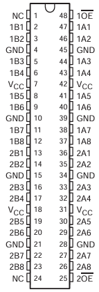
Pin Configuration and Descriptions
The SN74CBT16245 is available in a 48-pin TSSOP package. Below is the pin configuration and description:
Pin Configuration Table
| Pin Number | Pin Name | Description |
|---|---|---|
| 1 | 1OE | Output Enable for Bus 1 (Active Low) |
| 2-9 | 1A1-1A8 | Data Inputs/Outputs for Bus 1 (Side A) |
| 10 | GND | Ground |
| 11-18 | 2A1-2A8 | Data Inputs/Outputs for Bus 2 (Side A) |
| 19 | 2OE | Output Enable for Bus 2 (Active Low) |
| 20 | VCC | Power Supply (4.0V to 5.5V) |
| 21-28 | 2B1-2B8 | Data Inputs/Outputs for Bus 2 (Side B) |
| 29 | GND | Ground |
| 30-37 | 1B1-1B8 | Data Inputs/Outputs for Bus 1 (Side B) |
| 38 | 1OE | Output Enable for Bus 1 (Active Low) |
| 39-46 | NC | No Connection |
| 47 | 2OE | Output Enable for Bus 2 (Active Low) |
| 48 | VCC | Power Supply (4.0V to 5.5V) |
Usage Instructions
How to Use the SN74CBT16245 in a Circuit
- Power Supply: Connect the VCC pin to a stable power source within the range of 4.0V to 5.5V. Connect the GND pins to the ground of the circuit.
- Bus Connections:
- Connect the A-side pins (1A1-1A8, 2A1-2A8) to one bus.
- Connect the B-side pins (1B1-1B8, 2B1-2B8) to the other bus.
- Output Enable Control:
- Use the 1OE and 2OE pins to enable or disable the respective buses. These pins are active low, meaning a logic LOW enables the bus, and a logic HIGH disables it.
- Signal Direction: The SN74CBT16245 is bidirectional, so data can flow in either direction between the A and B sides when the corresponding OE pin is active.
Important Considerations and Best Practices
- Voltage Compatibility: Ensure that the logic levels of the connected buses are compatible with the SN74CBT16245's supported voltage range.
- Decoupling Capacitors: Place decoupling capacitors (e.g., 0.1µF) close to the VCC pin to stabilize the power supply and reduce noise.
- Unused Pins: Leave unused data pins floating or tie them to ground through a pull-down resistor to avoid floating inputs.
- Thermal Management: Ensure adequate ventilation or heat dissipation if the device operates at high frequencies or in a warm environment.
Example: Connecting to an Arduino UNO
The SN74CBT16245 can be used to interface an Arduino UNO (3.3V logic) with a 5V peripheral. Below is an example code snippet for enabling data transfer:
// Arduino UNO Example: Controlling the SN74CBT16245

const int oePin1 = 2; // Connect Arduino pin 2 to 1OE
const int oePin2 = 3; // Connect Arduino pin 3 to 2OE

void setup() {
  pinMode(oePin1, OUTPUT); // Set OE pin 1 as output
  pinMode(oePin2, OUTPUT); // Set OE pin 2 as output

  // Enable both buses by setting OE pins LOW
  digitalWrite(oePin1, LOW); // Enable Bus 1
  digitalWrite(oePin2, LOW); // Enable Bus 2
}

void loop() {
  // Data transfer occurs automatically when OE pins are LOW
  // Add your application-specific code here
}
Troubleshooting and FAQs
Common Issues and Solutions
No Data Transfer Between Buses:
- Cause: Output Enable (OE) pins are not set correctly.
- Solution: Ensure that the OE pins are set to logic LOW to enable the buses.
Signal Degradation or Noise:
- Cause: Poor PCB layout or lack of decoupling capacitors.
- Solution: Use proper PCB design practices and place decoupling capacitors near the VCC pin.
Device Overheating:
- Cause: Excessive current draw or high ambient temperature.
- Solution: Check the current requirements of connected devices and ensure proper ventilation.
Incorrect Voltage Levels:
- Cause: Mismatch between the logic levels of connected devices.
- Solution: Verify that the connected buses operate within the SN74CBT16245's supported voltage range.
FAQs
Q1: Can the SN74CBT16245 be used for level shifting between 3.3V and 5V systems?
A1: Yes, the SN74CBT16245 supports both 3.3V and 5V logic levels, making it suitable for level shifting applications.
Q2: What is the maximum data rate supported by the SN74CBT16245?
A2: The device supports high-speed data transfer with a typical propagation delay of 250ps, enabling operation in high-frequency systems.
Q3: Can I leave the OE pins floating if I don't need to control them?
A3: No, the OE pins should not be left floating. Tie them to ground (LOW) to enable the buses or to VCC (HIGH) to disable them.
Q4: Is the SN74CBT16245 suitable for bidirectional communication?
A4: Yes, the SN74CBT16245 is designed for bidirectional data transfer between two buses.