
How to Use 74VHC4052: Examples, Pinouts, and Specs
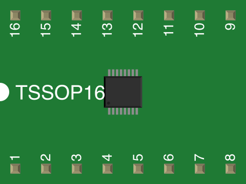
 Design with 74VHC4052 in Cirkit Designer
Introduction
The 74VHC4052 is a dual 4-channel analog multiplexer/demultiplexer manufactured by Nexperia (Part ID: 74VHC4052FT). This component enables the selection of one of several input signals to be routed to a single output, or vice versa, in analog signal processing applications. It is designed for high-speed operation and low-voltage environments, making it ideal for modern electronic systems.
Explore Projects Built with 74VHC4052
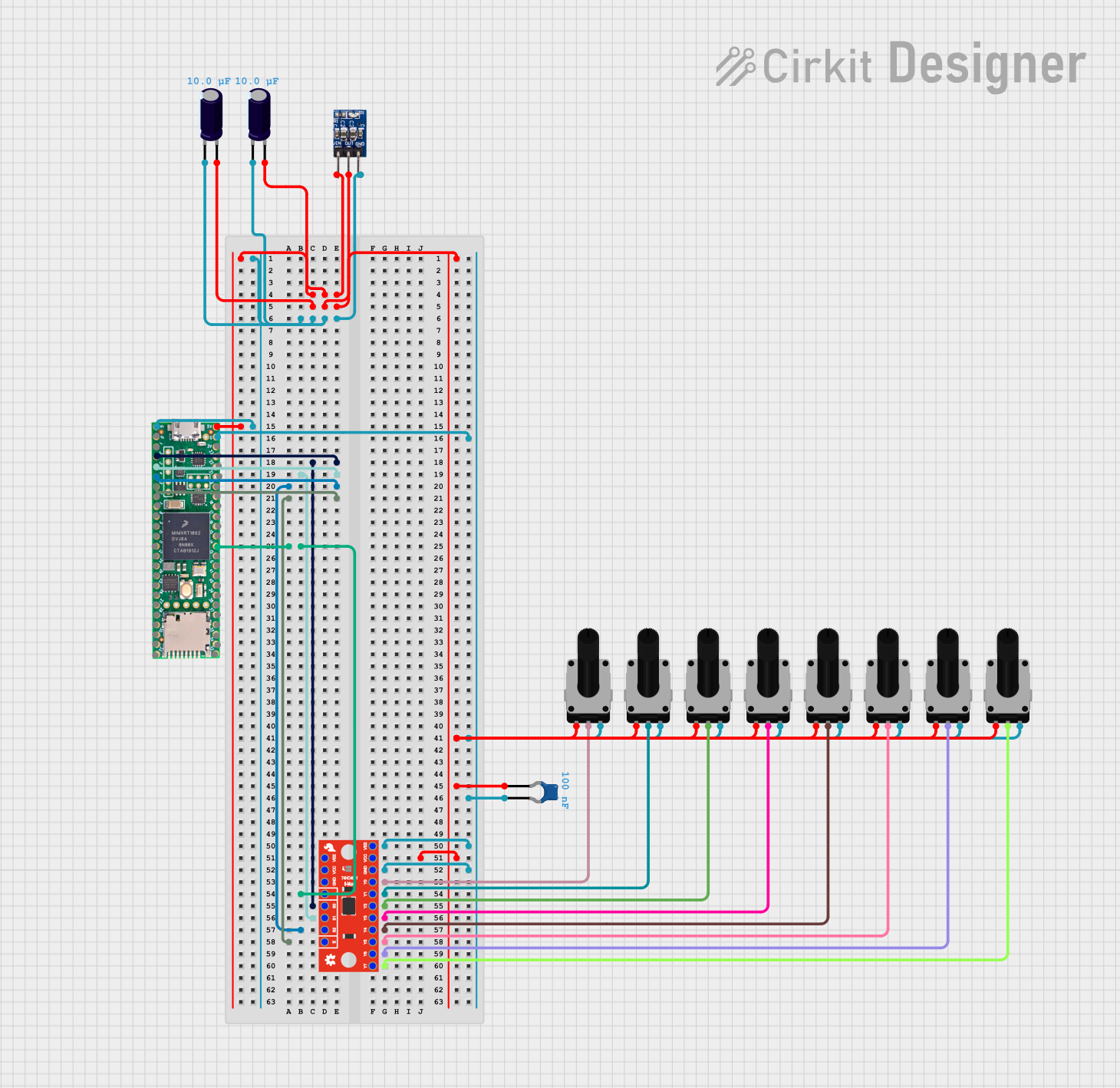 Open Project in Cirkit Designer
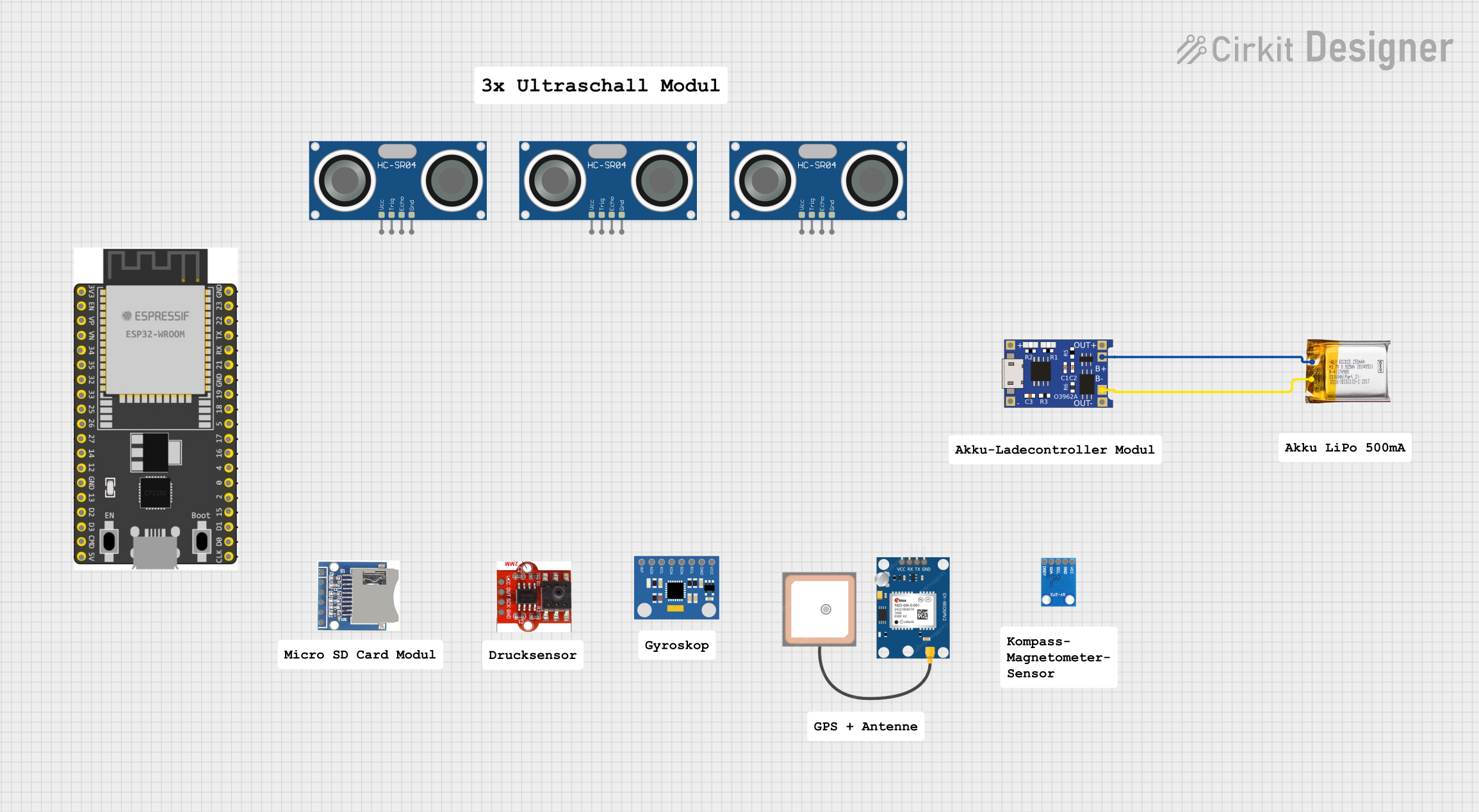 Open Project in Cirkit Designer
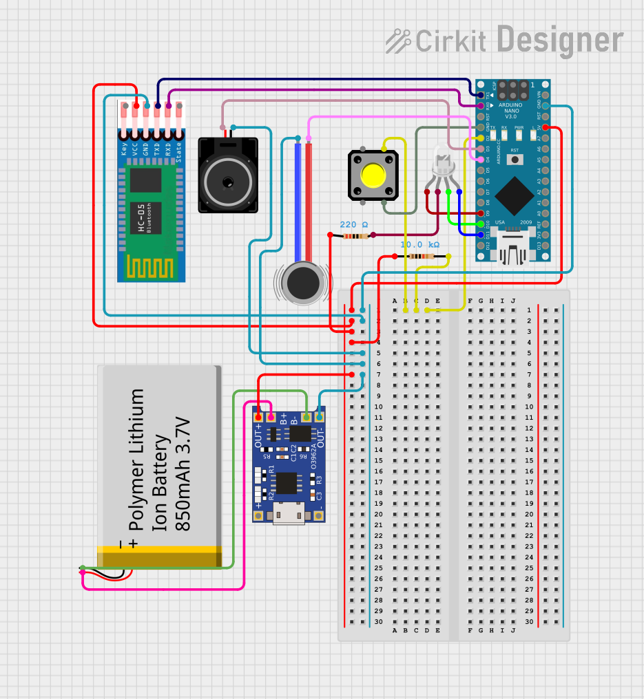 Open Project in Cirkit Designer
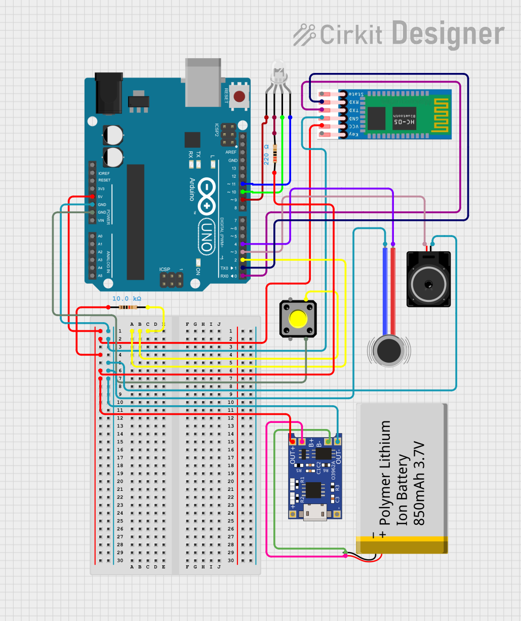 Open Project in Cirkit Designer
Explore Projects Built with 74VHC4052
Open Project in Cirkit DesignerOpen Project in Cirkit DesignerOpen Project in Cirkit DesignerOpen Project in Cirkit DesignerCommon Applications
- Audio signal routing
- Sensor signal multiplexing
- Data acquisition systems
- Analog-to-digital converter (ADC) input selection
- Communication systems
Technical Specifications
Key Technical Details
| Parameter | Value |
|---|---|
| Supply Voltage (Vcc) | 2.0 V to 5.5 V |
| Input Voltage Range | 0 V to Vcc |
| On-Resistance (Ron) | 70 Ω (typical at Vcc = 5 V) |
| Propagation Delay | 4 ns (typical at Vcc = 5 V) |
| Maximum Switching Frequency | 100 MHz |
| Operating Temperature Range | -40°C to +85°C |
| Package Type | TSSOP-16, SOIC-16 |
Pin Configuration and Descriptions
The 74VHC4052 comes in a 16-pin package. Below is the pinout and description:
| Pin No. | Name | Description |
|---|---|---|
| 1 | X0 | Channel 0 of multiplexer X |
| 2 | X1 | Channel 1 of multiplexer X |
| 3 | X2 | Channel 2 of multiplexer X |
| 4 | X3 | Channel 3 of multiplexer X |
| 5 | COMX | Common output/input for multiplexer X |
| 6 | COMY | Common output/input for multiplexer Y |
| 7 | Y3 | Channel 3 of multiplexer Y |
| 8 | Y2 | Channel 2 of multiplexer Y |
| 9 | Y1 | Channel 1 of multiplexer Y |
| 10 | Y0 | Channel 0 of multiplexer Y |
| 11 | INH | Inhibit pin (active HIGH, disables all channels when HIGH) |
| 12 | A | Select line A (used to select channels) |
| 13 | B | Select line B (used to select channels) |
| 14 | Vcc | Positive supply voltage |
| 15 | GND | Ground |
| 16 | VEE | Negative supply voltage (used for bipolar signal operation, typically GND) |
Usage Instructions
How to Use the 74VHC4052 in a Circuit
- Power Supply: Connect the Vcc pin to a voltage source within the range of 2.0 V to 5.5 V. Connect the GND pin to the ground of the circuit. If bipolar signals are used, connect VEE to the negative supply voltage; otherwise, connect it to GND.
- Channel Selection: Use the A and B select lines to choose the desired channel. The channel selection logic is as follows:
- A = 0, B = 0: Channel 0 is selected
- A = 1, B = 0: Channel 1 is selected
- A = 0, B = 1: Channel 2 is selected
- A = 1, B = 1: Channel 3 is selected
- Inhibit Function: When the INH pin is set HIGH, all channels are disabled, and no signal is passed through.
- Signal Routing: Connect the input signals to the Xn or Yn pins. The selected signal will be routed to the COMX or COMY pin, respectively.
Important Considerations and Best Practices
- Ensure that the input voltage does not exceed the supply voltage (Vcc) to avoid damage to the component.
- Use decoupling capacitors (e.g., 0.1 µF) near the Vcc pin to stabilize the power supply and reduce noise.
- For high-frequency signals, minimize trace lengths to reduce parasitic capacitance and signal degradation.
- If unused channels are present, connect them to GND to avoid floating inputs.
Example: Connecting to an Arduino UNO
The 74VHC4052 can be easily interfaced with an Arduino UNO for digital control of the multiplexer. Below is an example code snippet:
// Define control pins for the 74VHC4052
const int pinA = 2;  // Connect to A (pin 12 on 74VHC4052)
const int pinB = 3;  // Connect to B (pin 13 on 74VHC4052)
const int pinINH = 4; // Connect to INH (pin 11 on 74VHC4052)

void setup() {
  // Set control pins as outputs
  pinMode(pinA, OUTPUT);
  pinMode(pinB, OUTPUT);
  pinMode(pinINH, OUTPUT);

  // Enable the multiplexer by setting INH LOW
  digitalWrite(pinINH, LOW);
}

void loop() {
  // Example: Cycle through all channels
  for (int channel = 0; channel < 4; channel++) {
    // Set the select lines based on the channel
    digitalWrite(pinA, channel & 0x01); // LSB of channel
    digitalWrite(pinB, (channel >> 1) & 0x01); // MSB of channel

    // Wait for 1 second before switching to the next channel
    delay(1000);
  }
}
Troubleshooting and FAQs
Common Issues
No Signal Output:
- Ensure the INH pin is set to LOW to enable the multiplexer.
- Verify that the correct channel is selected using the A and B pins.
- Check the power supply connections (Vcc, GND, and VEE).
Signal Distortion:
- Ensure the input signal voltage is within the specified range (0 V to Vcc).
- Minimize trace lengths and use proper shielding for high-frequency signals.
Component Overheating:
- Verify that the input signals do not exceed the supply voltage.
- Check for short circuits or excessive current draw in the circuit.
FAQs
Q1: Can the 74VHC4052 handle digital signals?
Yes, the 74VHC4052 can handle both analog and digital signals, provided the signal levels are within the specified voltage range.
Q2: What is the purpose of the VEE pin?
The VEE pin allows the component to operate with bipolar signals. For unipolar operation, connect VEE to GND.
Q3: How do I reduce crosstalk between channels?
To minimize crosstalk, ensure proper grounding, use short traces, and avoid routing high-frequency signals near the multiplexer.
Q4: Can I use the 74VHC4052 with a 3.3 V system?
Yes, the 74VHC4052 is compatible with supply voltages as low as 2.0 V, making it suitable for 3.3 V systems.