How to Use ADS1292r: Examples, Pinouts, and Specs
Introduction
The ADS1292R, manufactured by Texas Instruments, is a low-power, 24-bit analog-to-digital converter (ADC) specifically designed for biopotential measurements. It is widely used in applications such as electrocardiogram (ECG) and electroencephalogram (EEG) monitoring. This component integrates programmable gain amplifiers (PGAs), a low-noise front-end, and supports multiple channels for simultaneous data acquisition, making it ideal for medical and wearable devices.
Explore Projects Built with ADS1292r
Explore Projects Built with ADS1292r
Common Applications
- Electrocardiogram (ECG) monitoring
- Electroencephalogram (EEG) monitoring
- Wearable health devices
- Patient monitoring systems
- Portable medical instruments
Technical Specifications
Key Technical Details
| Parameter | Value |
|---|---|
| Resolution | 24-bit |
| Number of Channels | 2 (simultaneous sampling) |
| Input Voltage Range | ±2.4 V (with internal reference) |
| Programmable Gain | 1, 2, 3, 4, 6, 8, or 12 |
| Data Rate | 125 SPS to 32 kSPS |
| Power Supply Voltage | 2.7 V to 5.25 V |
| Power Consumption | 335 µW (typical, at 3 V and 500 SPS) |
| Communication Interface | SPI |
| Operating Temperature Range | -40°C to +85°C |
| Package Type | TQFN-28 |
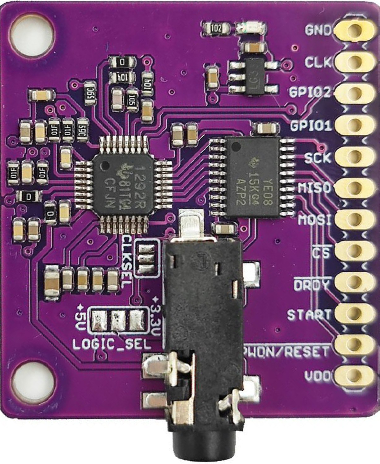
Pin Configuration and Descriptions
The ADS1292R comes in a 28-pin TQFN package. Below is the pin configuration:
| Pin Number | Pin Name | Description |
|---|---|---|
| 1 | DVDD | Digital power supply (1.8 V to 3.6 V) |
| 2 | DGND | Digital ground |
| 3 | START | Start signal input to begin conversions |
| 4 | CS | Chip select for SPI communication |
| 5 | SCLK | Serial clock input for SPI |
| 6 | DIN | Serial data input for SPI |
| 7 | DOUT | Serial data output for SPI |
| 8 | DRDY | Data ready output signal |
| 9 | RESET | Active-low reset input |
| 10 | CLKSEL | Clock source selection (internal or external) |
| 11 | PWDN | Power-down mode input |
| 12 | AVDD | Analog power supply (2.7 V to 5.25 V) |
| 13 | AGND | Analog ground |
| 14-15 | IN1P, IN1N | Positive and negative inputs for Channel 1 |
| 16-17 | IN2P, IN2N | Positive and negative inputs for Channel 2 |
| 18 | REFOUT | Reference voltage output |
| 19 | REFIN | Reference voltage input |
| 20 | VCAP1 | Decoupling capacitor connection for internal circuitry |
| 21 | VCAP2 | Decoupling capacitor connection for internal circuitry |
| 22-28 | NC | No connection |
Usage Instructions
How to Use the ADS1292R in a Circuit
- Power Supply: Connect the analog (AVDD) and digital (DVDD) power supplies within the specified range (2.7 V to 5.25 V for AVDD and 1.8 V to 3.6 V for DVDD). Ensure proper decoupling capacitors are placed near the power pins.
- Clock Source: Select the clock source using the CLKSEL pin. Use an external clock or the internal oscillator as required.
- Input Signals: Connect the biopotential signals (e.g., ECG electrodes) to the differential input pins (IN1P/IN1N and IN2P/IN2N). Use appropriate filtering to reduce noise.
- SPI Communication: Interface the ADS1292R with a microcontroller or processor via the SPI pins (CS, SCLK, DIN, DOUT). Ensure proper timing and configuration of the SPI interface.
- Reference Voltage: Use the internal reference voltage or provide an external reference voltage through the REFIN pin.
- Start Conversion: Use the START pin to initiate conversions. Monitor the DRDY pin to check when data is ready for retrieval.
Important Considerations and Best Practices
- Input Impedance: Ensure the input impedance of the connected circuit matches the ADS1292R's requirements to avoid signal degradation.
- Filtering: Use low-pass filters to remove high-frequency noise from the input signals.
- Grounding: Maintain a solid ground plane and separate analog and digital grounds to minimize noise.
- Power Supply Decoupling: Place decoupling capacitors (e.g., 0.1 µF and 10 µF) close to the power supply pins to reduce noise and ensure stable operation.
Example: Connecting ADS1292R to Arduino UNO
Below is an example of how to interface the ADS1292R with an Arduino UNO using SPI:
#include <SPI.h>

// Pin definitions for ADS1292R
#define CS_PIN 10  // Chip select pin
#define DRDY_PIN 9 // Data ready pin

void setup() {
  // Initialize SPI communication
  SPI.begin();
  pinMode(CS_PIN, OUTPUT);
  pinMode(DRDY_PIN, INPUT);
  digitalWrite(CS_PIN, HIGH); // Set CS high to deselect the device

  // Configure ADS1292R (example: reset and start conversion)
  resetADS1292R();
  startADS1292R();
}

void loop() {
  // Wait for data ready signal
  if (digitalRead(DRDY_PIN) == LOW) {
    digitalWrite(CS_PIN, LOW); // Select the ADS1292R
    uint8_t data = SPI.transfer(0x00); // Read data (example command)
    digitalWrite(CS_PIN, HIGH); // Deselect the ADS1292R

    // Process the received data
    Serial.println(data);
  }
}

void resetADS1292R() {
  // Send reset command to ADS1292R
  digitalWrite(CS_PIN, LOW);
  SPI.transfer(0x06); // Reset command
  digitalWrite(CS_PIN, HIGH);
  delay(10); // Wait for reset to complete
}

void startADS1292R() {
  // Send start command to ADS1292R
  digitalWrite(CS_PIN, LOW);
  SPI.transfer(0x08); // Start command
  digitalWrite(CS_PIN, HIGH);
}
Troubleshooting and FAQs
Common Issues and Solutions
No Data Output:
- Cause: SPI communication not configured correctly.
- Solution: Verify SPI clock polarity, phase, and speed settings. Ensure the CS pin is toggled correctly.
High Noise in Output:
- Cause: Poor grounding or insufficient filtering.
- Solution: Improve grounding and add low-pass filters to the input signals.
Device Not Responding:
- Cause: Incorrect power supply or reset sequence.
- Solution: Check power supply voltages and ensure the reset pin is toggled properly during initialization.
Incorrect Data:
- Cause: Mismatched reference voltage or input range.
- Solution: Verify the reference voltage and ensure the input signals are within the specified range.
FAQs
Can the ADS1292R operate with a single-ended input? No, the ADS1292R is designed for differential input signals. Single-ended inputs may result in degraded performance.
What is the maximum sampling rate? The ADS1292R supports a maximum data rate of 32 kSPS.
Can I use the internal oscillator as the clock source? Yes, the ADS1292R includes an internal oscillator that can be used as the clock source by setting the CLKSEL pin appropriately.