
How to Use YC164: Examples, Pinouts, and Specs

 Design with YC164 in Cirkit Designer
Introduction
The YC164 series, manufactured by Yageo, is a dual 4-bit static shift register designed for data storage and manipulation in digital circuits. This component is particularly useful for applications requiring serial data input and output, such as data transfer, signal processing, and digital communication systems. Its compact design and reliable performance make it a popular choice in embedded systems and microcontroller-based projects.
Explore Projects Built with YC164
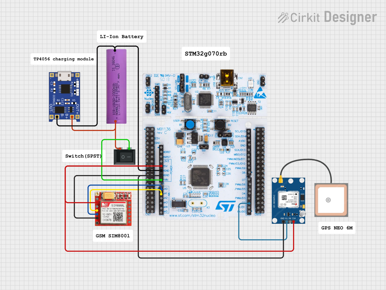 Open Project in Cirkit Designer
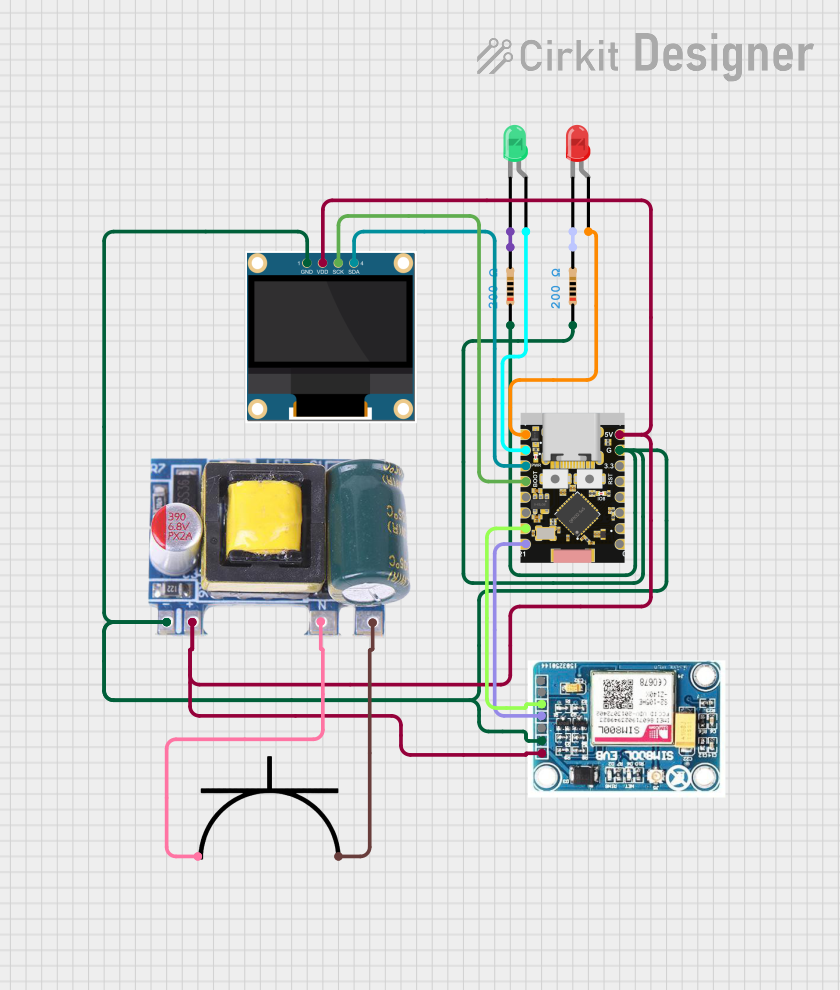 Open Project in Cirkit Designer
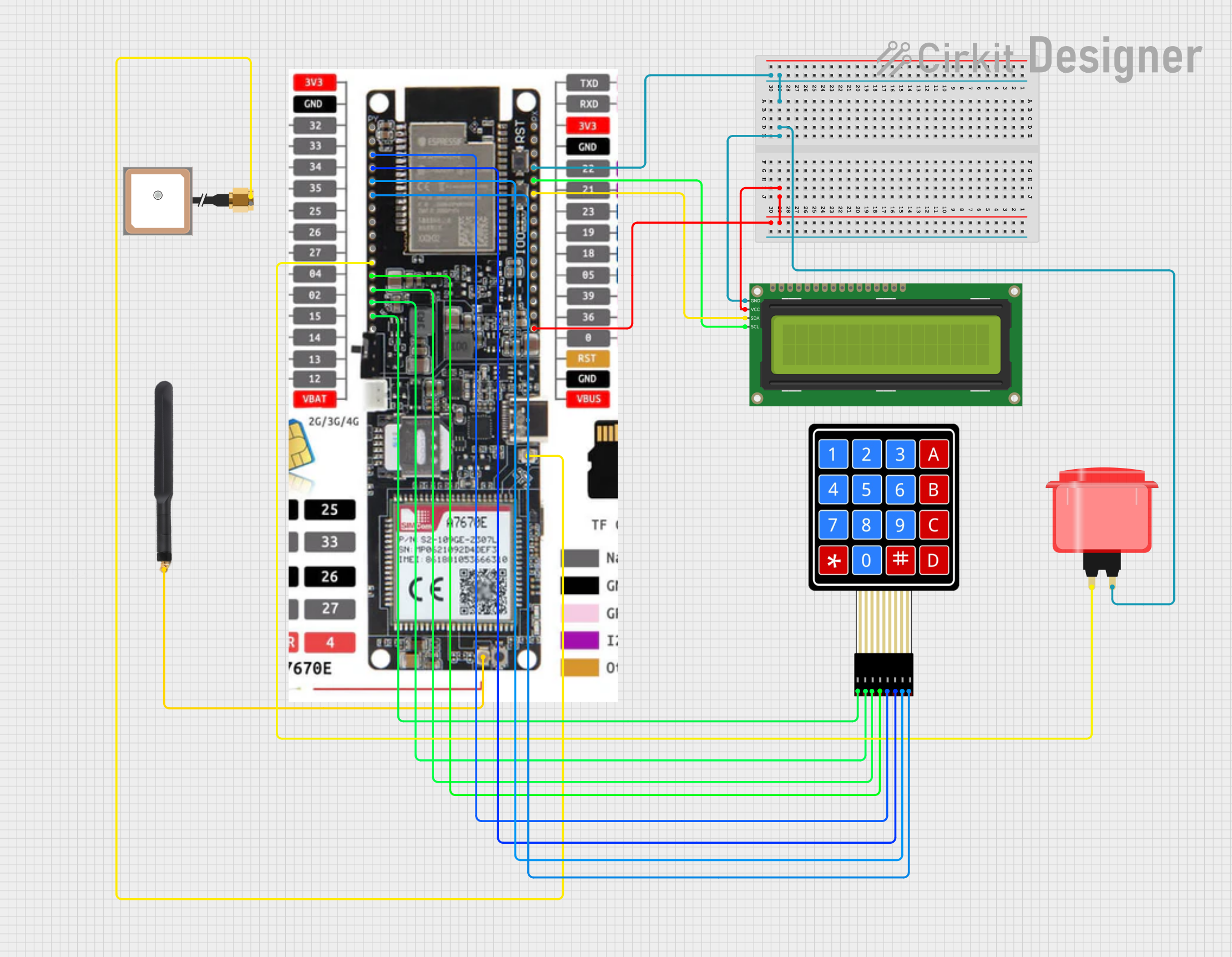 Open Project in Cirkit Designer
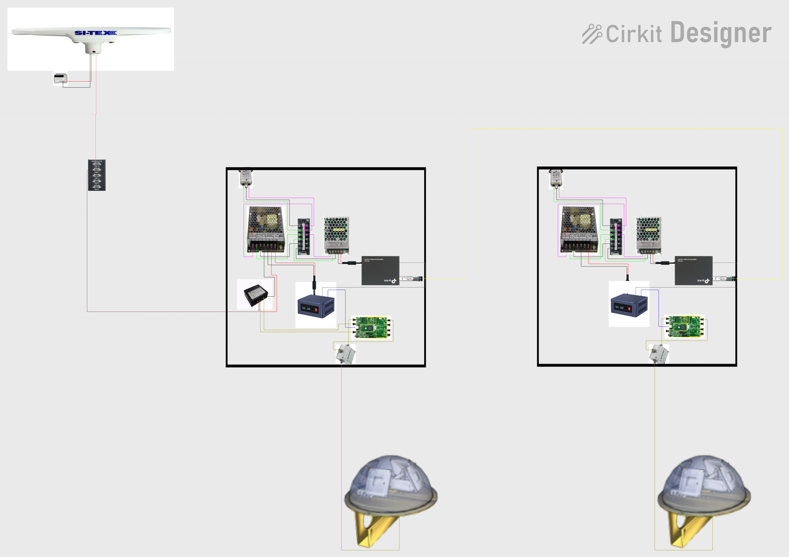 Open Project in Cirkit Designer
Explore Projects Built with YC164
Open Project in Cirkit DesignerOpen Project in Cirkit DesignerOpen Project in Cirkit DesignerOpen Project in Cirkit DesignerCommon Applications
- Serial-to-parallel or parallel-to-serial data conversion
- Data buffering and temporary storage
- Signal processing in digital systems
- Expanding I/O capabilities in microcontroller projects
- Digital communication systems
Technical Specifications
Key Technical Details
- Manufacturer Part ID: YC164 series
- Operating Voltage: 2.0V to 6.0V
- Maximum Clock Frequency: 25 MHz (at 5V supply)
- Input High Voltage (VIH): 2.0V (minimum at 5V supply)
- Input Low Voltage (VIL): 0.8V (maximum at 5V supply)
- Output High Voltage (VOH): 4.5V (minimum at 5V supply)
- Output Low Voltage (VOL): 0.5V (maximum at 5V supply)
- Operating Temperature Range: -40°C to +85°C
- Package Types: DIP, SOIC, TSSOP
Pin Configuration and Descriptions
The YC164 series has a 16-pin configuration. Below is the pinout and description:
| Pin Number | Pin Name | Description |
|---|---|---|
| 1 | VCC | Power supply (positive voltage) |
| 2 | SER1 | Serial data input for the first 4-bit register |
| 3 | CLK1 | Clock input for the first 4-bit register |
| 4 | Q1A | Output of the first bit in the first register |
| 5 | Q1B | Output of the second bit in the first register |
| 6 | Q1C | Output of the third bit in the first register |
| 7 | Q1D | Output of the fourth bit in the first register |
| 8 | GND | Ground (0V) |
| 9 | Q2D | Output of the fourth bit in the second register |
| 10 | Q2C | Output of the third bit in the second register |
| 11 | Q2B | Output of the second bit in the second register |
| 12 | Q2A | Output of the first bit in the second register |
| 13 | CLK2 | Clock input for the second 4-bit register |
| 14 | SER2 | Serial data input for the second 4-bit register |
| 15 | CLR | Asynchronous clear input (active low) |
| 16 | VCC | Power supply (positive voltage) |
Usage Instructions
How to Use the YC164 in a Circuit
- Power Supply: Connect the VCC pin to a stable power source (2.0V to 6.0V) and the GND pin to ground.
- Data Input: Provide serial data to the SER1 and/or SER2 pins. Data is shifted into the registers on the rising edge of the respective clock signals (CLK1 and CLK2).
- Clock Signal: Apply a clock signal to CLK1 and/or CLK2 to control the shifting of data. Ensure the clock frequency does not exceed 25 MHz at 5V supply.
- Outputs: The outputs (Q1A-Q1D and Q2A-Q2D) represent the current state of the registers. These can be used for further processing or interfacing with other components.
- Clear Function: To reset the registers, apply a low signal to the CLR pin. This will asynchronously clear all bits in both registers.
Important Considerations
- Ensure the input voltage levels (VIH and VIL) are within the specified range to avoid malfunction.
- Use decoupling capacitors (e.g., 0.1 µF) near the VCC pin to stabilize the power supply.
- Avoid exceeding the maximum clock frequency to maintain reliable operation.
- If unused, tie unused inputs (e.g., SER1, SER2) to a defined logic level (high or low) to prevent floating inputs.
Example: Connecting YC164 to an Arduino UNO
The following example demonstrates how to use the YC164 with an Arduino UNO to shift data into the first 4-bit register and display the output.
// Define pin connections
const int SER1 = 2;  // Serial data input for the first register
const int CLK1 = 3;  // Clock input for the first register
const int CLR = 4;   // Clear input (active low)

// Function to send a single bit to the YC164
void shiftBit(bool bitValue) {
  digitalWrite(SER1, bitValue);  // Set the data input
  digitalWrite(CLK1, HIGH);      // Generate a clock pulse
  delayMicroseconds(10);         // Short delay for stability
  digitalWrite(CLK1, LOW);       // End the clock pulse
}

void setup() {
  // Initialize pins
  pinMode(SER1, OUTPUT);
  pinMode(CLK1, OUTPUT);
  pinMode(CLR, OUTPUT);

  // Clear the register
  digitalWrite(CLR, LOW);  // Activate clear
  delay(10);               // Wait for the clear to take effect
  digitalWrite(CLR, HIGH); // Deactivate clear
}

void loop() {
  // Example: Shift the binary value 1010 into the register
  shiftBit(1);  // Shift in the first bit (MSB)
  shiftBit(0);  // Shift in the second bit
  shiftBit(1);  // Shift in the third bit
  shiftBit(0);  // Shift in the fourth bit (LSB)

  delay(1000);  // Wait for 1 second before repeating
}
Troubleshooting and FAQs
Common Issues
No Output on Q Pins:
- Ensure the clock signal is applied to the CLK pins.
- Verify that the SER pins are receiving valid data.
- Check the power supply connections (VCC and GND).
Registers Not Clearing:
- Confirm that the CLR pin is pulled low to activate the clear function.
- Ensure the CLR pin is not floating when inactive.
Erratic Behavior:
- Check for noise or instability in the clock signal.
- Use decoupling capacitors to stabilize the power supply.
FAQs
Q: Can I use the YC164 with a 3.3V microcontroller?
A: Yes, the YC164 operates within a voltage range of 2.0V to 6.0V, making it compatible with 3.3V systems.
Q: What happens if I exceed the maximum clock frequency?
A: Exceeding the maximum clock frequency may result in unreliable data shifting and incorrect outputs.
Q: Can I cascade multiple YC164 chips for longer shift registers?
A: Yes, you can cascade multiple YC164 chips by connecting the output of one register to the input of the next.