How to Use SN74AHCT125N : Examples, Pinouts, and Specs
Introduction
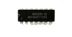
The SN74AHCT125N is a quad buffer/driver with 3-state outputs, manufactured by Texas Instruments. It is designed for high-speed operation and low power consumption, making it ideal for use in digital circuits. Each of the four independent buffers features a 3-state output, which can be controlled via an enable pin. This component is commonly used for signal buffering, level shifting, and driving high-capacitance loads in digital systems.
Explore Projects Built with SN74AHCT125N
Explore Projects Built with SN74AHCT125N
Common Applications
- Signal buffering in digital circuits
- Level shifting between different voltage domains
- Driving high-capacitance loads
- Bus interface and control in microcontroller-based systems
- Data communication and signal isolation
Technical Specifications
Key Technical Details
- Manufacturer Part ID: SN74AHCT125N
- Operating Voltage Range: 4.5 V to 5.5 V
- Input Voltage Range: 0 V to 5.5 V
- Output Voltage Range: 0 V to Vcc
- High-Level Input Voltage (VIH): 2.0 V (minimum)
- Low-Level Input Voltage (VIL): 0.8 V (maximum)
- Output Current (IO): ±25 mA (maximum per output)
- Quiescent Current (ICC): 8 µA (maximum)
- Propagation Delay: 6 ns (typical at 5 V)
- Operating Temperature Range: -40°C to 125°C
- Package Type: 14-pin PDIP (Plastic Dual In-line Package)
Pin Configuration and Descriptions
The SN74AHCT125N is a 14-pin IC with the following pinout:
| Pin Number | Pin Name | Description |
|---|---|---|
| 1 | 1OE | Output Enable for Buffer 1 (Active LOW) |
| 2 | 1A | Input for Buffer 1 |
| 3 | 1Y | Output for Buffer 1 |
| 4 | 2OE | Output Enable for Buffer 2 (Active LOW) |
| 5 | 2A | Input for Buffer 2 |
| 6 | 2Y | Output for Buffer 2 |
| 7 | GND | Ground |
| 8 | 3Y | Output for Buffer 3 |
| 9 | 3A | Input for Buffer 3 |
| 10 | 3OE | Output Enable for Buffer 3 (Active LOW) |
| 11 | 4Y | Output for Buffer 4 |
| 12 | 4A | Input for Buffer 4 |
| 13 | 4OE | Output Enable for Buffer 4 (Active LOW) |
| 14 | VCC | Power Supply (4.5 V to 5.5 V) |
Usage Instructions
How to Use the SN74AHCT125N in a Circuit
- Power Supply: Connect the VCC pin (Pin 14) to a 5 V power supply and the GND pin (Pin 7) to ground.
- Input Signals: Apply the input signals to the
Apins (Pins 2, 5, 9, and 12) of the respective buffers. - Output Enable Control: Use the
OEpins (Pins 1, 4, 10, and 13) to control the 3-state outputs:- Drive the
OEpin LOW to enable the corresponding output. - Drive the
OEpin HIGH to place the output in a high-impedance (Hi-Z) state.
- Drive the
- Output Signals: The buffered output signals will appear on the
Ypins (Pins 3, 6, 8, and 11) when the correspondingOEpin is LOW.
Important Considerations and Best Practices
- Ensure that the input voltage levels are within the specified range (0 V to 5.5 V).
- Avoid exceeding the maximum output current of ±25 mA per output to prevent damage to the IC.
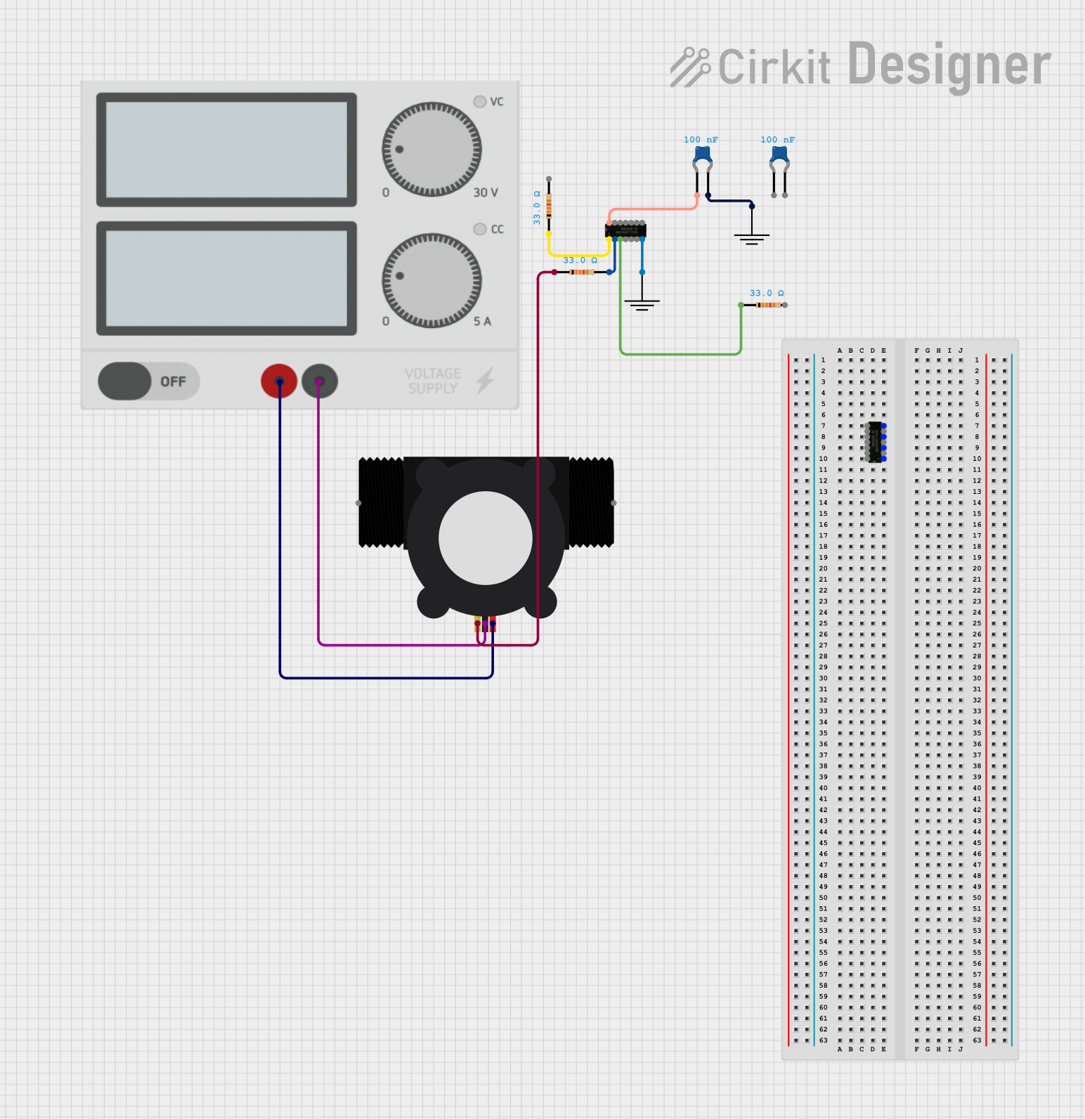
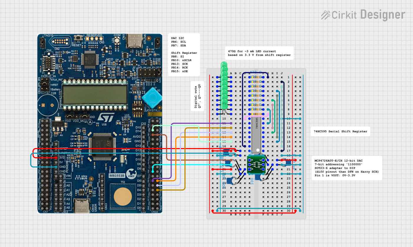
- Use decoupling capacitors (e.g., 0.1 µF) near the VCC pin to stabilize the power supply and reduce noise.
- When using the 3-state outputs, ensure that no two outputs are connected directly to avoid bus contention.
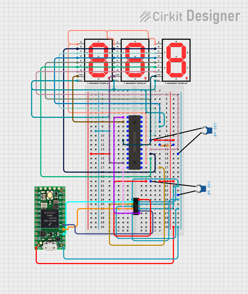
Example: Connecting the SN74AHCT125N to an Arduino UNO
The following example demonstrates how to use the SN74AHCT125N to buffer a digital signal from an Arduino UNO.
Circuit Connections
- Connect the VCC pin (Pin 14) to the Arduino's 5 V pin and the GND pin (Pin 7) to the Arduino's GND.
- Connect an Arduino digital output pin (e.g., Pin 8) to the
1Apin (Pin 2) of the SN74AHCT125N. - Connect the
1OEpin (Pin 1) to GND to enable the output. - Connect the
1Ypin (Pin 3) to the desired load or circuit.
Arduino Code
// Example code to demonstrate the use of SN74AHCT125N with Arduino UNO

void setup() {
  pinMode(8, OUTPUT); // Set Pin 8 as an output to drive the SN74AHCT125N
}

void loop() {
  digitalWrite(8, HIGH); // Send a HIGH signal to the buffer input
  delay(1000);           // Wait for 1 second
  digitalWrite(8, LOW);  // Send a LOW signal to the buffer input
  delay(1000);           // Wait for 1 second
}
Troubleshooting and FAQs
Common Issues and Solutions
No Output Signal:
- Ensure that the
OEpin for the corresponding buffer is connected to GND (LOW). - Verify that the input signal is within the specified voltage range.
- Ensure that the
Output Signal is Distorted:
- Check for excessive load capacitance on the output pin. If necessary, reduce the load or use a series resistor.
- Ensure proper decoupling of the power supply using capacitors near the VCC pin.
High Current Consumption:
- Verify that no two outputs are shorted together or connected to conflicting signals.
- Check for any floating input pins and connect them to a defined logic level (HIGH or LOW).
Component Overheating:
- Ensure that the output current does not exceed the maximum rating of ±25 mA per output.
- Verify that the power supply voltage is within the specified range (4.5 V to 5.5 V).
FAQs
Q1: Can the SN74AHCT125N be used for level shifting?
A1: Yes, the SN74AHCT125N can be used for level shifting from TTL (3.3 V) to CMOS (5 V) logic levels, as it is designed to be compatible with TTL input levels.
Q2: What happens if the OE pin is left floating?
A2: If the OE pin is left floating, the output state is undefined. Always connect the OE pin to a defined logic level (HIGH or LOW).
Q3: Can multiple outputs be connected together?
A3: Yes, but only if the outputs are in a high-impedance (Hi-Z) state. Otherwise, connecting active outputs together can cause bus contention and damage the IC.
Q4: Is the SN74AHCT125N suitable for driving LEDs?
A4: The SN74AHCT125N can drive LEDs, but ensure that the current through the LED does not exceed the maximum output current rating of ±25 mA. Use a current-limiting resistor in series with the LED.