
How to Use CY7C64215: Examples, Pinouts, and Specs
 Design with CY7C64215 in Cirkit Designer
Introduction
The CY7C64215, manufactured by Infineon Technologies, is a high-speed, low-power, 16-bit programmable logic device (PLD) designed for a wide range of digital applications. Its flexible architecture enables users to implement custom logic configurations, making it ideal for creating complex digital functions. This component is particularly useful in applications such as signal processing, data routing, and custom digital control systems.
Explore Projects Built with CY7C64215
 Open Project in Cirkit Designer
 Open Project in Cirkit Designer
 Open Project in Cirkit Designer
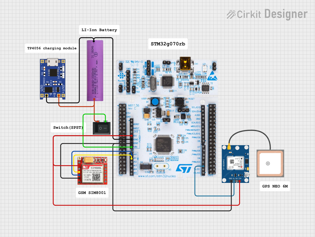 Open Project in Cirkit Designer
Explore Projects Built with CY7C64215
Open Project in Cirkit DesignerOpen Project in Cirkit DesignerOpen Project in Cirkit DesignerOpen Project in Cirkit DesignerCommon Applications
- Digital signal processing
- Data routing and multiplexing
- Custom logic implementation
- Embedded system design
- Industrial automation and control systems
Technical Specifications
Key Technical Details
| Parameter | Value |
|---|---|
| Manufacturer | Infineon Technologies |
| Part Number | CY7C64215 |
| Logic Type | Programmable Logic Device (PLD) |
| Architecture | 16-bit |
| Operating Voltage Range | 1.8V to 3.3V |
| Maximum Clock Frequency | 100 MHz |
| Power Consumption | Low Power |
| I/O Pins | 24 |
| Package Type | QFN-32, TQFP-44 |
| Operating Temperature Range | -40°C to +85°C |
Pin Configuration and Descriptions
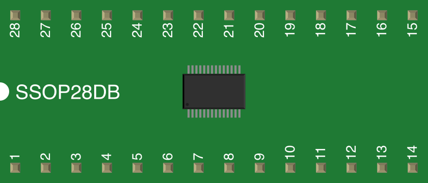
The CY7C64215 is available in multiple package types. Below is the pin configuration for the QFN-32 package:
| Pin Number | Pin Name | Description |
|---|---|---|
| 1 | VCC | Power supply (1.8V to 3.3V) |
| 2 | GND | Ground |
| 3-10 | IO1-IO8 | General-purpose input/output pins |
| 11 | CLK | Clock input for synchronous operations |
| 12 | RESET | Active-low reset input |
| 13-20 | IO9-IO16 | General-purpose input/output pins |
| 21 | VREF | Reference voltage for analog/digital operations |
| 22-29 | IO17-IO24 | General-purpose input/output pins |
| 30 | TEST | Test mode pin (leave unconnected in normal use) |
| 31 | CONFIG | Configuration pin for programming |
| 32 | NC | No connection |
Usage Instructions
How to Use the CY7C64215 in a Circuit
- Power Supply: Connect the VCC pin to a stable power source within the range of 1.8V to 3.3V. Connect the GND pin to the circuit ground.
- Clock Input: Provide a clock signal to the CLK pin if synchronous operation is required.
- Reset: Use the RESET pin to initialize the device. This pin is active-low, so pull it low to reset the device.
- I/O Pins: Configure the I/O pins (IO1-IO24) as inputs or outputs based on your application. These pins can be programmed for custom logic functions.
- Programming: Use the CONFIG pin to program the device with your desired logic configuration. A compatible programmer or development tool is required.
- Bypass Capacitors: Place decoupling capacitors (e.g., 0.1 µF) near the VCC pin to reduce noise and ensure stable operation.
Important Considerations and Best Practices
- Voltage Levels: Ensure that all input signals are within the specified voltage range to avoid damage to the device.
- Unused Pins: Leave unused I/O pins unconnected or tie them to ground through a pull-down resistor.
- Thermal Management: If operating in high-temperature environments, ensure proper heat dissipation to maintain reliability.
- Programming: Use Infineon’s recommended programming tools and software to configure the device.
Example: Connecting CY7C64215 to an Arduino UNO
The CY7C64215 can be interfaced with an Arduino UNO for custom logic control. Below is an example of how to toggle an LED connected to one of the I/O pins of the CY7C64215.
Arduino Code Example
// Define the pin connected to the CY7C64215 I/O pin
const int cy7c64215Pin = 7; // Arduino pin connected to CY7C64215 IO1

void setup() {
  pinMode(cy7c64215Pin, OUTPUT); // Set the pin as an output
}

void loop() {
  digitalWrite(cy7c64215Pin, HIGH); // Turn on the LED
  delay(1000); // Wait for 1 second
  digitalWrite(cy7c64215Pin, LOW);  // Turn off the LED
  delay(1000); // Wait for 1 second
}
Note: Ensure proper voltage level shifting if the Arduino operates at 5V, as the CY7C64215 operates at a maximum of 3.3V.
Troubleshooting and FAQs
Common Issues and Solutions
Device Not Responding
- Cause: Incorrect power supply or missing connections.
- Solution: Verify that the VCC and GND pins are properly connected and the supply voltage is within the specified range.
Programming Failure
- Cause: Incorrect programming tool or configuration.
- Solution: Use Infineon’s recommended programming tools and ensure the CONFIG pin is properly connected.
Unexpected Behavior
- Cause: Noise or unstable clock signal.
- Solution: Use decoupling capacitors near the power pins and ensure a stable clock source.
Overheating
- Cause: Excessive current draw or poor thermal management.
- Solution: Check the circuit for shorts and ensure proper heat dissipation.
FAQs
Q1: Can the CY7C64215 be reprogrammed?
Yes, the CY7C64215 is a programmable logic device and can be reprogrammed multiple times using compatible tools.
Q2: What is the maximum clock frequency supported?
The CY7C64215 supports a maximum clock frequency of 100 MHz.
Q3: Can I use the CY7C64215 in a 5V system?
The CY7C64215 operates at a maximum voltage of 3.3V. Use level shifters if interfacing with a 5V system.
Q4: What happens if the RESET pin is left floating?
Leaving the RESET pin floating may cause unpredictable behavior. It is recommended to pull it high using a pull-up resistor when not in use.
Q5: Are there any development boards available for the CY7C64215?
Infineon provides development kits and evaluation boards for the CY7C64215. Check their official website for availability.