How to Use AD9850: Examples, Pinouts, and Specs
Introduction
The AD9850 is a highly versatile direct digital synthesizer (DDS) capable of generating both sine and square waveforms with exceptional frequency resolution. It operates from a single power supply and supports output frequencies up to 40 MHz. The AD9850 is widely used in applications such as signal generation, frequency modulation, waveform synthesis, and communication systems. Its compact design and high performance make it a popular choice for hobbyists and professionals alike.
Explore Projects Built with AD9850
Explore Projects Built with AD9850
Common Applications:
- Signal generators for testing and measurement
- Frequency modulation and demodulation
- Local oscillators in communication systems
- Function generators for waveform synthesis
- Amateur radio and RF projects
Technical Specifications
Below are the key technical details of the AD9850:
| Parameter | Value |
|---|---|
| Supply Voltage | 2.7 V to 5.5 V |
| Output Frequency Range | 0 Hz to 40 MHz |
| Frequency Resolution | 0.0291 Hz (32-bit tuning word) |
| Output Waveforms | Sine wave, Square wave |
| Power Consumption | ~380 mW at 5 V |
| Communication Interface | Parallel or Serial (SPI-like) |
| Clock Input Frequency | Up to 125 MHz |
| Operating Temperature Range | -40°C to +85°C |
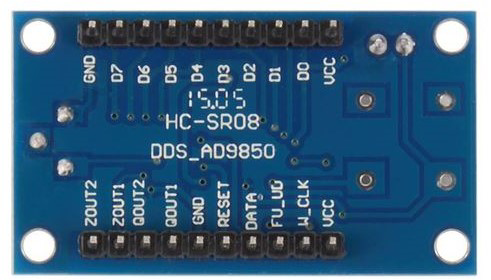
Pin Configuration and Descriptions
The AD9850 is typically available in a 28-pin SOIC package. Below is the pinout and description:
| Pin Number | Pin Name | Description |
|---|---|---|
| 1 | W_CLK | Clock input for frequency tuning word updates |
| 2 | FQ_UD | Frequency update; latches tuning word into DDS core |
| 3 | DATA | Serial data input for frequency and phase control |
| 4 | RESET | Resets the DDS to its default state |
| 5-12 | D0-D7 | Parallel data input pins (used in parallel mode) |
| 13 | GND | Ground connection |
| 14 | VCC | Power supply input (2.7 V to 5.5 V) |
| 15 | CLK IN | External clock input (up to 125 MHz) |
| 16 | IOUT | Current output for sine wave (requires external load resistor) |
| 17 | IOUTB | Complementary current output |
| 18 | REF OUT | Reference clock output |
| 19 | REF IN | Reference clock input |
| 20-28 | NC | No connection (reserved for future use) |
Usage Instructions
How to Use the AD9850 in a Circuit
- Power Supply: Connect the VCC pin to a stable power source (2.7 V to 5.5 V) and the GND pin to ground.
- Clock Input: Provide a stable clock signal to the CLK IN pin. A 125 MHz crystal oscillator is commonly used.
- Waveform Output: Connect a load resistor (typically 200 Ω) between the IOUT and GND pins to generate a sine wave. For square wave output, use the onboard comparator.
- Control Interface: Use either the serial (SPI-like) or parallel interface to program the frequency, phase, and waveform type. The serial interface is more commonly used due to its simplicity.
Example: Connecting AD9850 to Arduino UNO
The AD9850 can be easily controlled using an Arduino UNO via the serial interface. Below is an example code to generate a 1 MHz sine wave:
// Include necessary libraries
#include <SPI.h>

// Define AD9850 control pins
#define W_CLK 8   // Word load clock pin
#define FQ_UD 9   // Frequency update pin
#define DATA 10   // Serial data pin
#define RESET 11  // Reset pin

// Function to send a 40-bit word to the AD9850
void sendWord(uint32_t frequencyWord) {
  for (int i = 0; i < 32; i++) {
    digitalWrite(DATA, (frequencyWord & 0x01)); // Send LSB first
    digitalWrite(W_CLK, HIGH);
    digitalWrite(W_CLK, LOW);
    frequencyWord >>= 1; // Shift to the next bit
  }
  // Send 8 control bits (all zeros for default settings)
  for (int i = 0; i < 8; i++) {
    digitalWrite(DATA, LOW);
    digitalWrite(W_CLK, HIGH);
    digitalWrite(W_CLK, LOW);
  }
  // Latch the frequency word into the DDS core
  digitalWrite(FQ_UD, HIGH);
  digitalWrite(FQ_UD, LOW);
}

void setup() {
  // Initialize control pins
  pinMode(W_CLK, OUTPUT);
  pinMode(FQ_UD, OUTPUT);
  pinMode(DATA, OUTPUT);
  pinMode(RESET, OUTPUT);

  // Reset the AD9850
  digitalWrite(RESET, HIGH);
  delay(10);
  digitalWrite(RESET, LOW);

  // Calculate the frequency tuning word for 1 MHz
  uint32_t tuningWord = (uint32_t)((1.0 * pow(2, 32)) / 125.0); // 125 MHz clock
  sendWord(tuningWord); // Send the tuning word to the AD9850
}

void loop() {
  // The AD9850 will continuously output the programmed frequency
}
Important Considerations:
- Use decoupling capacitors (e.g., 0.1 µF) near the VCC pin to reduce noise.
- Ensure the clock input signal is stable and within the specified range.
- Avoid exceeding the maximum output frequency of 40 MHz to prevent distortion.
- Use a heatsink or proper ventilation if operating at high frequencies for extended periods.
Troubleshooting and FAQs
Common Issues and Solutions
No Output Signal:
- Ensure the power supply is stable and within the specified range.
- Verify that the clock input signal is present and within the 125 MHz limit.
- Check the connections to the IOUT pin and ensure a proper load resistor is used.
Distorted Waveform:
- Verify that the output frequency does not exceed 40 MHz.
- Check for noise or instability in the power supply or clock input.
- Use proper shielding and grounding to minimize interference.
Incorrect Frequency Output:
- Double-check the frequency tuning word calculation.
- Ensure the serial or parallel interface is configured correctly.
FAQs
Q: Can the AD9850 generate square waves directly?
A: Yes, the AD9850 has an onboard comparator that can generate square waves from the sine wave output.
Q: What is the maximum clock input frequency?
A: The AD9850 supports clock input frequencies up to 125 MHz.
Q: Can I use the AD9850 with a 3.3 V microcontroller?
A: Yes, the AD9850 operates with a supply voltage as low as 2.7 V, making it compatible with 3.3 V systems.
Q: How do I calculate the frequency tuning word?
A: Use the formula: Tuning Word = (Desired Frequency * 2^32) / Clock Frequency.
By following this documentation, users can effectively integrate the AD9850 into their projects and troubleshoot common issues.