How to Use 74LS164: Examples, Pinouts, and Specs
Introduction
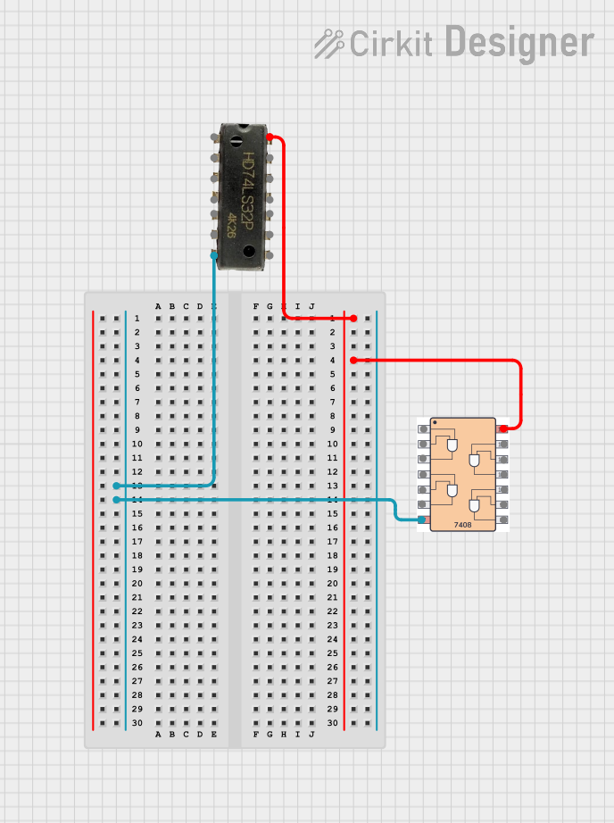
The 74LS164 is an 8-bit serial-in, parallel-out shift register. It is designed to convert serial data into parallel data, making it a versatile component in digital electronics. The device features two serial data inputs (A and B) and eight parallel outputs (Q0 to Q7). It operates on a clock signal, shifting data through its internal registers on each clock pulse. The 74LS164 is widely used in applications such as data storage, data transfer, digital signal processing, and LED driving.
Explore Projects Built with 74LS164
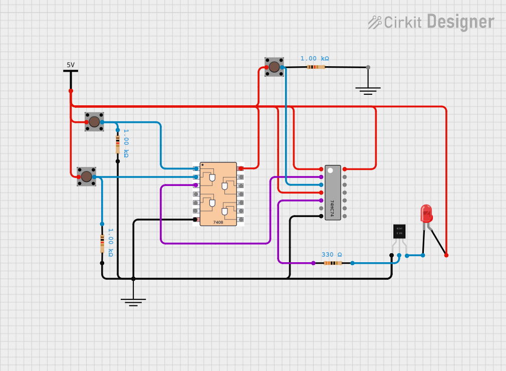
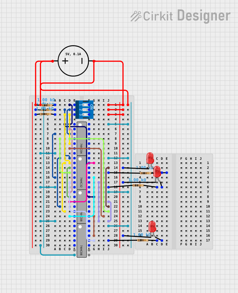
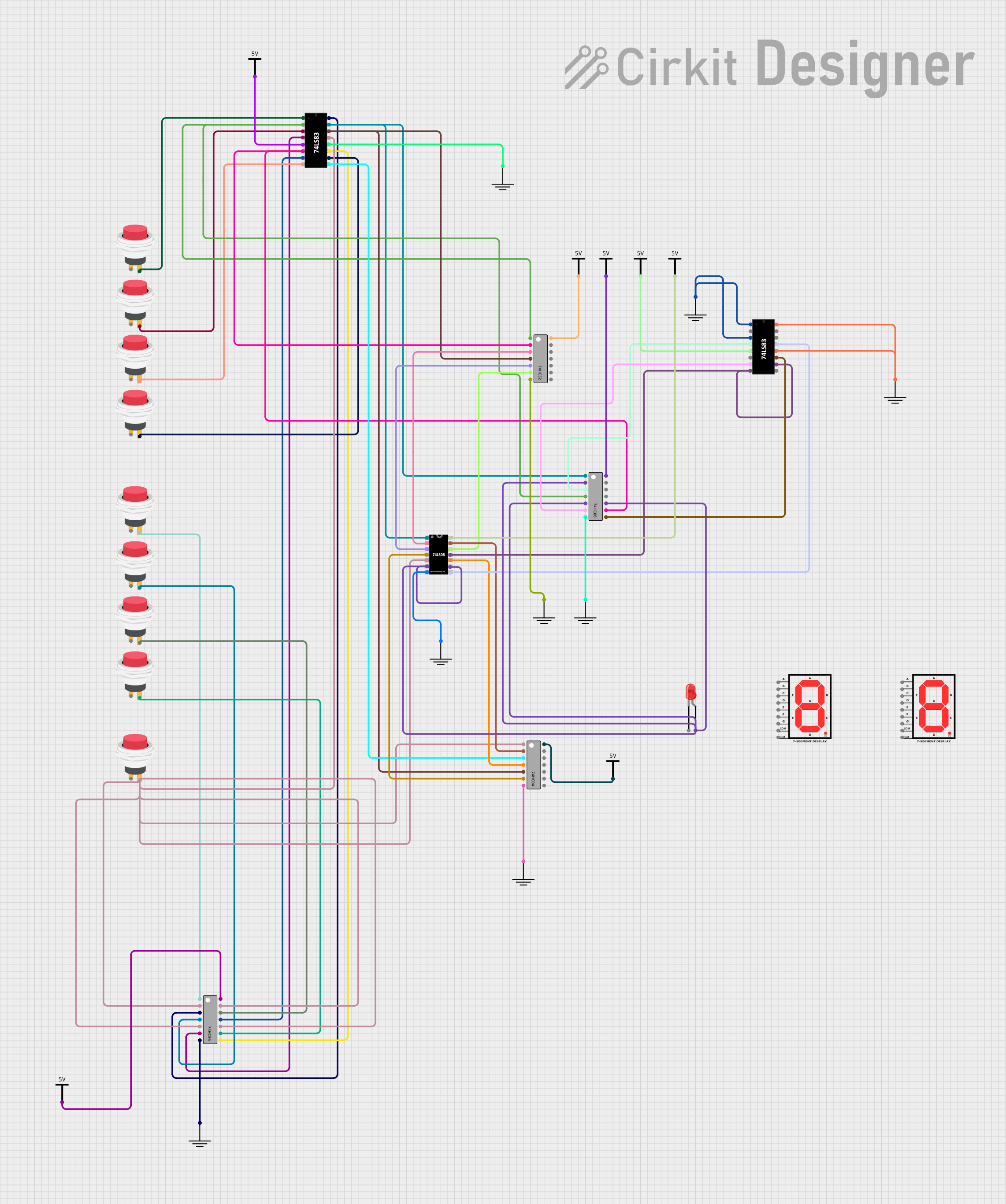
Explore Projects Built with 74LS164
Common Applications:
- Expanding microcontroller I/O pins
- Driving LED arrays or 7-segment displays
- Serial-to-parallel data conversion
- Digital signal processing
- Data buffering and storage
Technical Specifications
The following are the key technical details of the 74LS164:
| Parameter | Value |
|---|---|
| Supply Voltage (Vcc) | 4.75V to 5.25V |
| Input Voltage (VI) | 0V to 5.5V |
| High-Level Input Voltage | 2.0V (minimum) |
| Low-Level Input Voltage | 0.8V (maximum) |
| Maximum Clock Frequency | 25 MHz |
| Output Current (per pin) | 8 mA |
| Propagation Delay | 22 ns (typical) |
| Operating Temperature | 0°C to 70°C |
| Package Types | DIP-14, SOIC-14 |
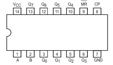
Pin Configuration and Descriptions
The 74LS164 comes in a 14-pin package. The pinout and descriptions are as follows:
| Pin Number | Pin Name | Description |
|---|---|---|
| 1 | A | Serial Data Input A |
| 2 | B | Serial Data Input B |
| 3 | Q0 | Parallel Output Bit 0 |
| 4 | Q1 | Parallel Output Bit 1 |
| 5 | Q2 | Parallel Output Bit 2 |
| 6 | Q3 | Parallel Output Bit 3 |
| 7 | GND | Ground (0V) |
| 8 | Q4 | Parallel Output Bit 4 |
| 9 | Q5 | Parallel Output Bit 5 |
| 10 | Q6 | Parallel Output Bit 6 |
| 11 | Q7 | Parallel Output Bit 7 |
| 12 | CLK | Clock Input (Rising Edge Triggered) |
| 13 | CLR | Asynchronous Clear (Active Low) |
| 14 | Vcc | Positive Supply Voltage |
Usage Instructions
How to Use the 74LS164 in a Circuit
- Power Supply: Connect the Vcc pin (14) to a 5V power supply and the GND pin (7) to ground.
- Data Input: Use the A and/or B pins (1 and 2) to input serial data. These inputs are ANDed together, so at least one must be HIGH for data to shift.
- Clock Signal: Provide a clock signal to the CLK pin (12). Data is shifted on the rising edge of the clock.
- Clear Function: To reset the shift register, pull the CLR pin (13) LOW. This clears all outputs (Q0 to Q7) to LOW.
- Parallel Outputs: Connect the Q0 to Q7 pins (3 to 6, 8 to 11) to the desired load (e.g., LEDs, microcontroller inputs).
Important Considerations and Best Practices
- Pull-Up Resistors: Use pull-up resistors on the CLR pin to ensure it remains HIGH during normal operation.
- Clock Signal: Ensure the clock signal is clean and free of noise to avoid unintended shifts.
- Output Loading: Do not exceed the maximum output current of 8 mA per pin to prevent damage.
- Bypass Capacitor: Place a 0.1 µF decoupling capacitor near the Vcc pin to stabilize the power supply.
Example: Connecting the 74LS164 to an Arduino UNO
The following example demonstrates how to use the 74LS164 to drive an 8-LED array with an Arduino UNO.
Circuit Connections:
- Connect the 74LS164's Vcc to the Arduino's 5V pin and GND to GND.
- Connect the CLK pin to Arduino digital pin 8.
- Connect the A pin to Arduino digital pin 9.
- Connect the CLR pin to Arduino digital pin 10.
- Connect Q0 to Q7 to the LED array (with current-limiting resistors).
Arduino Code:
// Define pin connections
const int dataPin = 9;  // Serial data input (A)
const int clockPin = 8; // Clock input (CLK)
const int clearPin = 10; // Clear input (CLR)

// Function to send a byte of data to the 74LS164
void shiftOutData(byte data) {
  for (int i = 0; i < 8; i++) {
    // Send each bit (MSB first)
    digitalWrite(dataPin, (data & (1 << (7 - i))) ? HIGH : LOW);
    digitalWrite(clockPin, HIGH); // Pulse the clock
    delayMicroseconds(10);        // Short delay for stability
    digitalWrite(clockPin, LOW);
  }
}

void setup() {
  // Set pin modes
  pinMode(dataPin, OUTPUT);
  pinMode(clockPin, OUTPUT);
  pinMode(clearPin, OUTPUT);

  // Initialize the 74LS164
  digitalWrite(clearPin, HIGH); // Keep CLR HIGH for normal operation
  digitalWrite(clockPin, LOW);  // Initialize clock to LOW
}

void loop() {
  // Example: Light up LEDs in a binary counting pattern
  for (byte i = 0; i < 256; i++) {
    shiftOutData(i); // Send data to the 74LS164
    delay(500);      // Wait for 500ms
  }
}
Troubleshooting and FAQs
Common Issues and Solutions
Outputs Not Changing:
- Ensure the clock signal is connected and functioning properly.
- Verify that the CLR pin is HIGH during normal operation.
- Check the serial data inputs (A and B) for proper logic levels.
Flickering Outputs:
- Add a decoupling capacitor (0.1 µF) near the Vcc pin to reduce power supply noise.
- Ensure the clock signal is free of jitter or noise.
No Output on Q Pins:
- Verify that the Vcc and GND connections are secure.
- Check if the maximum clock frequency (25 MHz) is being exceeded.
FAQs
Q: Can I cascade multiple 74LS164 ICs for more outputs?
A: Yes, you can cascade multiple 74LS164 ICs by connecting the Q7 output of one IC to the serial data input (A or B) of the next IC.
Q: What happens if both A and B inputs are LOW?
A: If both A and B are LOW, no data will be shifted into the register, and the outputs will remain unchanged.
Q: Can the 74LS164 drive high-power loads directly?
A: No, the 74LS164 cannot drive high-power loads directly. Use external transistors or drivers for such applications.