
How to Use W25QXX: Examples, Pinouts, and Specs
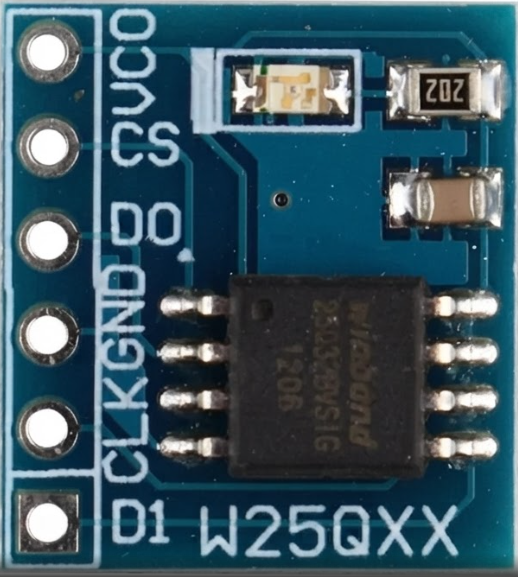
 Design with W25QXX in Cirkit Designer
Introduction
The W25QXX series, manufactured by Winbond, is a family of high-performance serial NOR flash memory chips that utilize the SPI (Serial Peripheral Interface) protocol for communication. These chips are designed for data storage in embedded systems, offering fast read/write speeds, low power consumption, and a wide range of memory capacities to suit various applications.
Explore Projects Built with W25QXX
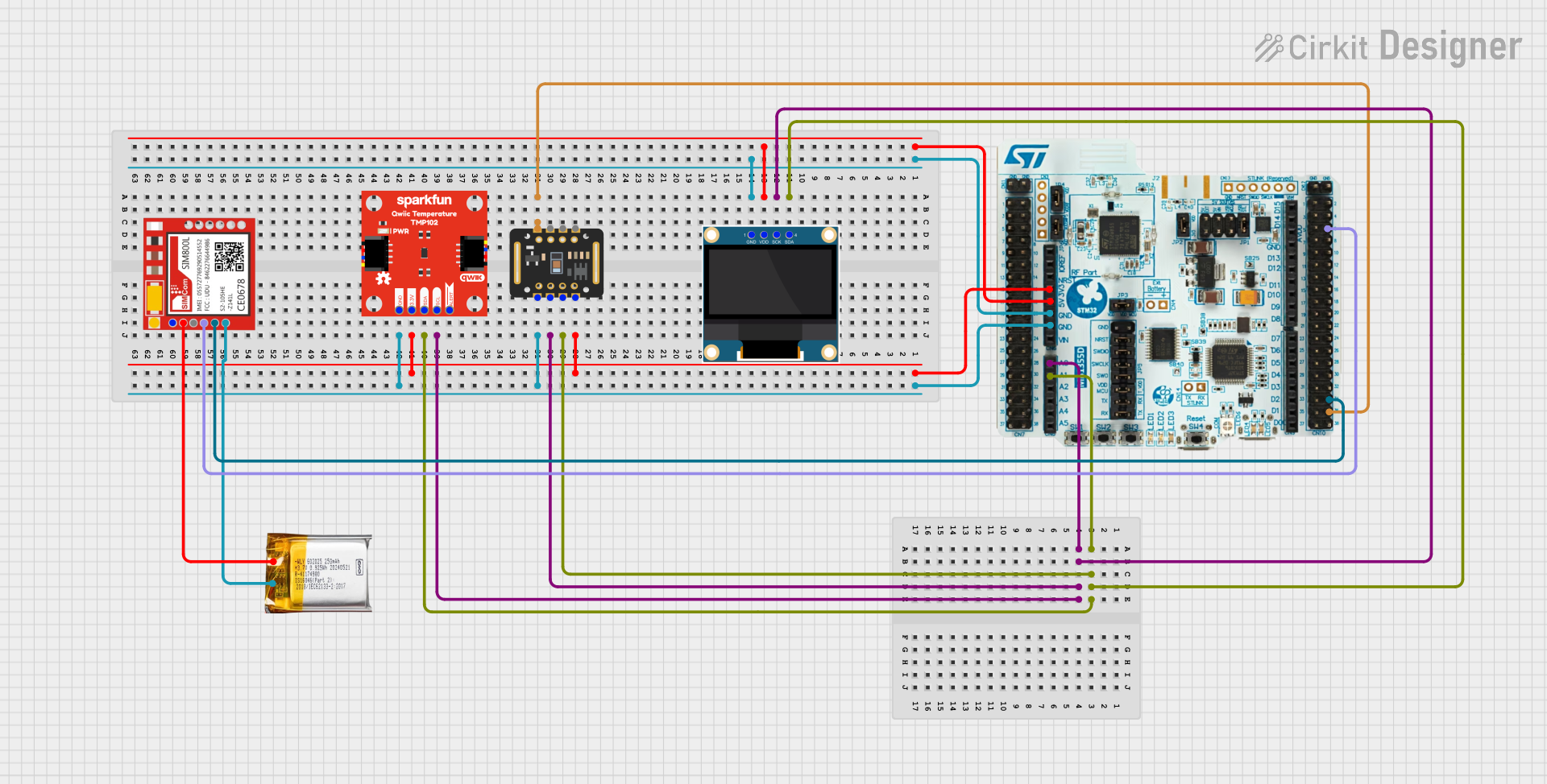 Open Project in Cirkit Designer
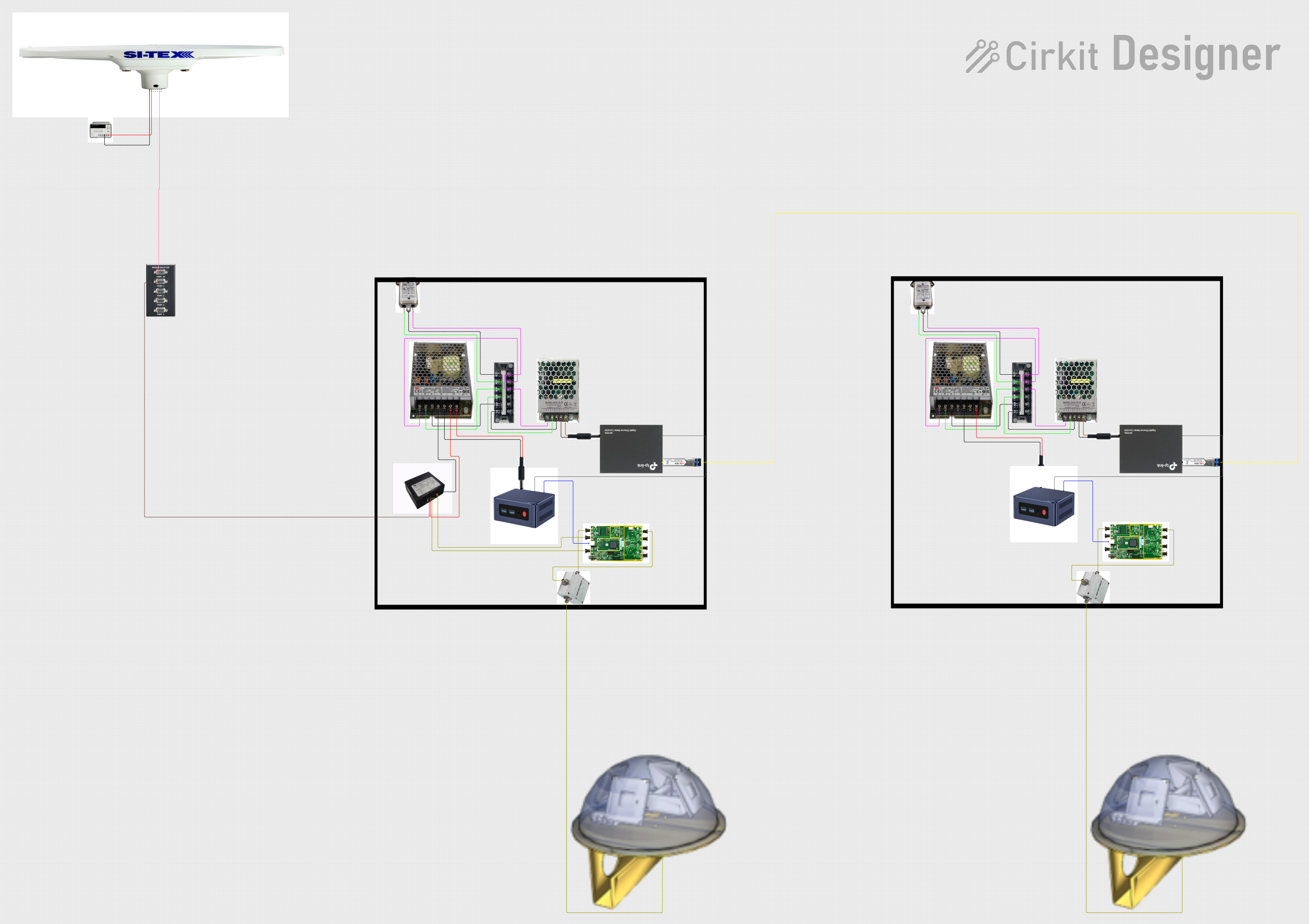 Open Project in Cirkit Designer
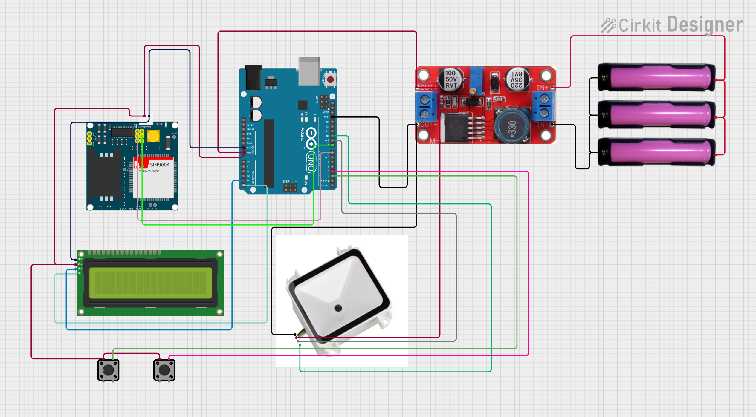 Open Project in Cirkit Designer
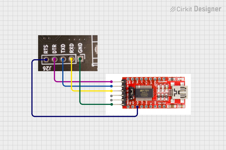 Open Project in Cirkit Designer
Explore Projects Built with W25QXX
Open Project in Cirkit DesignerOpen Project in Cirkit DesignerOpen Project in Cirkit DesignerOpen Project in Cirkit DesignerCommon Applications and Use Cases
- Firmware storage for microcontrollers and embedded systems
- Data logging in IoT devices
- Boot memory for systems requiring fast startup
- Storage for multimedia files in portable devices
- Code shadowing for high-speed execution in processors
Technical Specifications
The W25Q128FV is a specific member of the W25QXX series, offering 128 Mbit (16 MB) of storage capacity. Below are the key technical details:
Key Specifications
| Parameter | Value |
|---|---|
| Memory Capacity | 128 Mbit (16 MB) |
| Interface | SPI (Serial Peripheral Interface) |
| Operating Voltage | 2.7V to 3.6V |
| Maximum Clock Frequency | 104 MHz (Standard SPI) |
| Page Size | 256 bytes |
| Sector Size | 4 KB |
| Block Size | 64 KB |
| Erase Cycles | 100,000 cycles (typical) |
| Data Retention | 20 years |
| Operating Temperature | -40°C to +85°C |
| Package Options | SOP-8, WSON-8, USON-8, and others |
Pin Configuration and Descriptions
The W25Q128FV is typically available in an 8-pin package. Below is the pinout and description:
| Pin No. | Pin Name | Description |
|---|---|---|
| 1 | CS# | Chip Select (Active Low). Enables communication with the device. |
| 2 | DO (MISO) | Data Output (Master In Slave Out). Transfers data from the chip to the host. |
| 3 | WP# | Write Protect (Active Low). Protects specific memory regions from writing. |
| 4 | GND | Ground. Connect to system ground. |
| 5 | DI (MOSI) | Data Input (Master Out Slave In). Transfers data from the host to the chip. |
| 6 | CLK | Clock. Synchronizes data transfer between the host and the chip. |
| 7 | HOLD# | Hold (Active Low). Pauses communication without deselecting the chip. |
| 8 | VCC | Power Supply. Connect to a 2.7V–3.6V power source. |
Usage Instructions
How to Use the W25Q128FV in a Circuit
- Power Supply: Connect the VCC pin to a 3.3V power source and the GND pin to ground.
- SPI Connections: Connect the SPI pins (CS#, CLK, DI, DO) to the corresponding SPI pins on your microcontroller or host device.
- Optional Pins:
- Connect WP# to VCC if write protection is not required.
- Connect HOLD# to VCC if the hold function is not needed.
- Pull-Up Resistors: Use pull-up resistors on CS#, WP#, and HOLD# pins if required by your design.
- Initialization: Configure the SPI interface on your microcontroller to match the W25Q128FV's SPI mode (Mode 0 or Mode 3).
Important Considerations and Best Practices
- Voltage Levels: Ensure the SPI signals are within the operating voltage range (2.7V–3.6V).
- Clock Speed: Operate within the maximum clock frequency of 104 MHz for reliable communication.
- Erase Before Write: Always erase a sector or block before writing new data to it.
- Data Retention: Store critical data in multiple locations to account for potential wear over time.
- Decoupling Capacitor: Place a 0.1 µF decoupling capacitor near the VCC pin to stabilize the power supply.
Example Code for Arduino UNO
Below is an example of interfacing the W25Q128FV with an Arduino UNO using the SPI library:
#include <SPI.h>

// Pin definitions for the W25Q128FV
#define CS_PIN 10  // Chip Select pin connected to Arduino pin 10

void setup() {
  // Initialize Serial Monitor
  Serial.begin(9600);

  // Initialize SPI
  SPI.begin();
  pinMode(CS_PIN, OUTPUT);
  digitalWrite(CS_PIN, HIGH); // Deselect the chip

  Serial.println("W25Q128FV Initialization Complete");
}

void loop() {
  // Example: Read Manufacturer ID
  digitalWrite(CS_PIN, LOW); // Select the chip
  SPI.transfer(0x90);        // Command to read Manufacturer ID
  SPI.transfer(0x00);        // Dummy byte 1
  SPI.transfer(0x00);        // Dummy byte 2
  SPI.transfer(0x00);        // Dummy byte 3
  byte manufacturerID = SPI.transfer(0x00); // Read Manufacturer ID
  digitalWrite(CS_PIN, HIGH); // Deselect the chip

  // Print Manufacturer ID
  Serial.print("Manufacturer ID: 0x");
  Serial.println(manufacturerID, HEX);

  delay(1000); // Wait for 1 second
}
Troubleshooting and FAQs
Common Issues and Solutions
No Response from the Chip:
- Ensure the CS# pin is correctly toggled (LOW to select, HIGH to deselect).
- Verify SPI connections and ensure the clock frequency is within the supported range.
Data Corruption:
- Check if the sector/block was erased before writing new data.
- Ensure stable power supply and proper decoupling.
Write Protection Not Working:
- Verify the WP# pin is correctly configured.
- Check the status register to ensure the write protection bits are set correctly.
Device Not Recognized:
- Confirm the SPI mode (Mode 0 or Mode 3) matches the microcontroller's configuration.
- Verify the manufacturer ID and device ID using the appropriate commands.
FAQs
Q: Can I use the W25Q128FV with a 5V microcontroller?
A: The W25Q128FV operates at 2.7V–3.6V. Use a level shifter or voltage divider to interface with 5V logic.
Q: How do I erase the entire chip?
A: Use the "Chip Erase" command (0xC7 or 0x60). Note that this operation can take several seconds.
Q: What is the difference between sectors and blocks?
A: Sectors are smaller (4 KB) and are ideal for frequent updates, while blocks are larger (64 KB) and suited for bulk data storage.
Q: How do I check if a write operation is complete?
A: Read the status register and check the Write-In-Progress (WIP) bit. Writing is complete when WIP = 0.