Cirkit Designer Logo
Cirkit Designer
Your all-in-one circuit design IDE
Home / 
Component Documentation

How to Use 74HC08: Examples, Pinouts, and Specs

Image of 74HC08
Cirkit Designer LogoDesign with 74HC08 in Cirkit Designer

Introduction

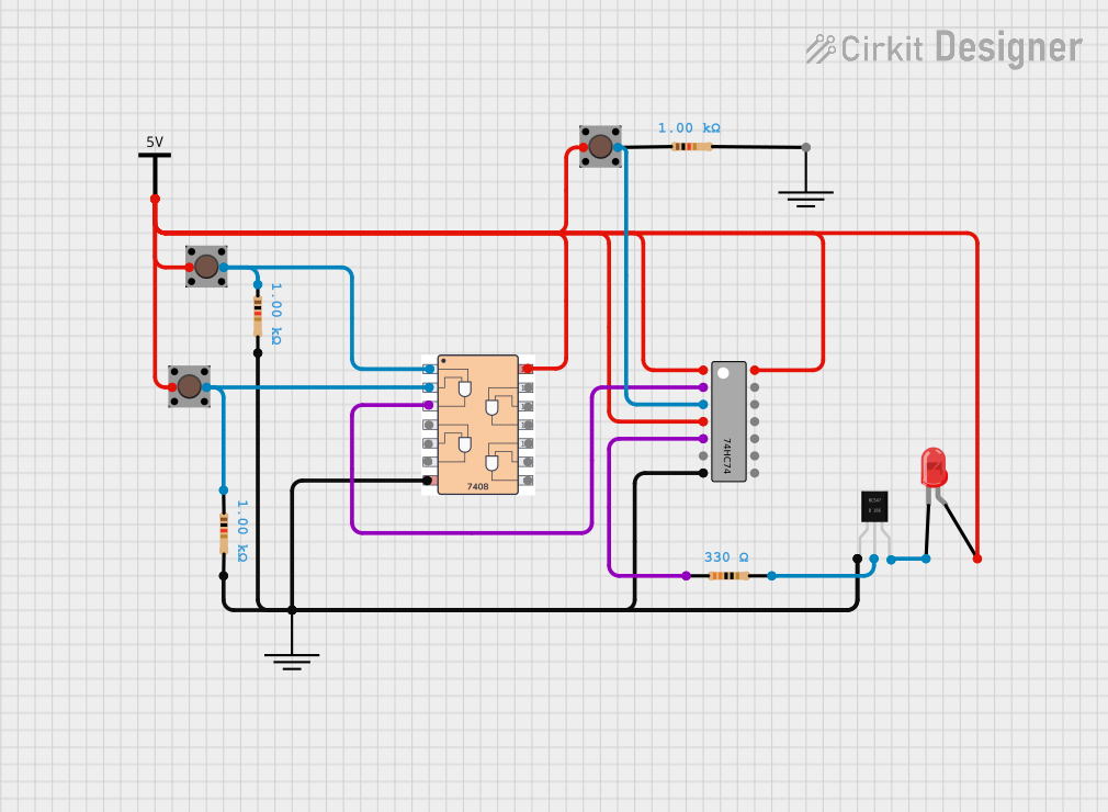
The 74HC08 integrated circuit is a high-speed Si-gate CMOS device that contains four independent 2-input AND gates. This component is designed to operate from a wide range of power supply voltages and offers low power consumption, making it a popular choice for digital logic systems. Common applications include:

  • Logic gate functions in digital circuits
  • Signal gating
  • Input/output buffering
  • Building complex logic functions by combining multiple gates

Explore Projects Built with 74HC08

Use Cirkit Designer to design, explore, and prototype these projects online. Some projects support real-time simulation. Click "Open Project" to start designing instantly!
STM32-Controlled LED Display with 74HC595 Shift Register and 12-Bit DAC
Image of Harry Stim Breadboard: A project utilizing 74HC08 in a practical application
This circuit uses a 74HC595 shift register to control multiple LEDs via a common ground configuration, with a microcontroller providing serial data input. It includes decoupling capacitors for stability and a 12-Bit DAC, potentially for analog signal generation or reference voltage application.
Cirkit Designer LogoOpen Project in Cirkit Designer
Arduino Mega 2560-Based LED Control System with Logic Gates
Image of Lab 4: A project utilizing 74HC08 in a practical application
This circuit features an Arduino Mega 2560 microcontroller interfaced with multiple logic ICs (74HC04, 74HC08, 74HC32) to control a set of LEDs (red, green, blue) through resistors. The logic ICs perform various AND, OR, and NOT operations to drive the LEDs based on the microcontroller's inputs.
Cirkit Designer LogoOpen Project in Cirkit Designer
Logic Gate and Binary Adder Experimentation Board
Image of BCD to full adder and subtractor: A project utilizing 74HC08 in a practical application
This circuit is a digital logic system that likely performs arithmetic operations and logical processing based on user inputs from push switches. It includes binary full adders for arithmetic functions, various logic gates for processing signals, and output interfaces such as 7-segment displays and LEDs for displaying results or statuses.
Cirkit Designer LogoOpen Project in Cirkit Designer
74HC74 and 7408 Based LED Control Circuit with Push Switches
Image of Lab1: A project utilizing 74HC08 in a practical application
This circuit is a simple flip-flop based LED control system. It uses a 74HC74 D flip-flop to toggle the state of an LED, with push switches to control the clock and data inputs. The circuit also includes a 7408 AND gate and a BC547 transistor to drive the LED.
Cirkit Designer LogoOpen Project in Cirkit Designer

Explore Projects Built with 74HC08

Use Cirkit Designer to design, explore, and prototype these projects online. Some projects support real-time simulation. Click "Open Project" to start designing instantly!
Image of Harry Stim Breadboard: A project utilizing 74HC08 in a practical application
STM32-Controlled LED Display with 74HC595 Shift Register and 12-Bit DAC
This circuit uses a 74HC595 shift register to control multiple LEDs via a common ground configuration, with a microcontroller providing serial data input. It includes decoupling capacitors for stability and a 12-Bit DAC, potentially for analog signal generation or reference voltage application.
Cirkit Designer LogoOpen Project in Cirkit Designer
Image of Lab 4: A project utilizing 74HC08 in a practical application
Arduino Mega 2560-Based LED Control System with Logic Gates
This circuit features an Arduino Mega 2560 microcontroller interfaced with multiple logic ICs (74HC04, 74HC08, 74HC32) to control a set of LEDs (red, green, blue) through resistors. The logic ICs perform various AND, OR, and NOT operations to drive the LEDs based on the microcontroller's inputs.
Cirkit Designer LogoOpen Project in Cirkit Designer
Image of BCD to full adder and subtractor: A project utilizing 74HC08 in a practical application
Logic Gate and Binary Adder Experimentation Board
This circuit is a digital logic system that likely performs arithmetic operations and logical processing based on user inputs from push switches. It includes binary full adders for arithmetic functions, various logic gates for processing signals, and output interfaces such as 7-segment displays and LEDs for displaying results or statuses.
Cirkit Designer LogoOpen Project in Cirkit Designer
Image of Lab1: A project utilizing 74HC08 in a practical application
74HC74 and 7408 Based LED Control Circuit with Push Switches
This circuit is a simple flip-flop based LED control system. It uses a 74HC74 D flip-flop to toggle the state of an LED, with push switches to control the clock and data inputs. The circuit also includes a 7408 AND gate and a BC547 transistor to drive the LED.
Cirkit Designer LogoOpen Project in Cirkit Designer

Technical Specifications

Key Technical Details

  • Supply Voltage (Vcc): 2.0V to 6.0V
  • Input Voltage (Vin): 0V to Vcc
  • Output Voltage (Vout): 0V to Vcc
  • High-Level Input Voltage (VIH): Minimum 2V
  • Low-Level Input Voltage (VIL): Maximum 0.8V
  • High-Level Output Current (IOH): Maximum -5.2 mA
  • Low-Level Output Current (IOL): Maximum 5.2 mA
  • Propagation Delay Time: Approximately 8ns (at Vcc = 4.5V)
  • Operating Temperature Range: -40°C to +125°C

Pin Configuration and Descriptions

Pin Number Name Description
1 1A Input A for Gate 1
2 1B Input B for Gate 1
3 1Y Output for Gate 1
4 2A Input A for Gate 2
5 2B Input B for Gate 2
6 2Y Output for Gate 2
7 GND Ground (0V)
8 3A Input A for Gate 3
9 3B Input B for Gate 3
10 3Y Output for Gate 3
11 4A Input A for Gate 4
12 4B Input B for Gate 4
13 4Y Output for Gate 4
14 Vcc Positive Supply Voltage

Usage Instructions

How to Use the 74HC08 in a Circuit

  1. Connect the Vcc pin (14) to the positive supply voltage within the specified range (2.0V to 6.0V).
  2. Connect the GND pin (7) to the ground of the power supply.
  3. Apply input signals to the A and B inputs of the desired AND gate(s).
  4. The output Y of each gate will be HIGH only if both inputs A and B are HIGH.

Important Considerations and Best Practices

  • Ensure that the power supply voltage does not exceed the maximum rating to prevent damage.
  • Inputs should not be left floating; connect them to a defined logic level if not in use.
  • Use pull-up or pull-down resistors as needed to maintain input signal integrity.
  • Decoupling capacitors (typically 0.1 µF) should be placed close to the Vcc pin to filter out noise.

Troubleshooting and FAQs

Common Issues

  • Outputs not behaving as expected: Verify that all inputs are at valid logic levels and that the power supply is within the specified range.
  • Device heating up: Check for short circuits or supply voltage exceeding the maximum rating.

Solutions and Tips

  • Double-check wiring and ensure that inputs are not inadvertently shorted to Vcc or GND.
  • Use a multimeter to measure the supply voltage and input levels to ensure they are within the specified range.

FAQs

Q: Can I use the 74HC08 at a supply voltage lower than 2.0V? A: No, the device may not function correctly below the minimum supply voltage.

Q: What happens if I exceed the maximum input voltage? A: Exceeding the maximum input voltage can damage the device and lead to permanent failure.

Q: Can I connect the outputs of two gates together? A: No, connecting outputs directly can cause damage. Use an OR gate or diodes for wired-OR logic instead.

Example Code for Arduino UNO

The following example demonstrates how to use the 74HC08 with an Arduino UNO to perform a simple AND operation.

// Define the input and output pins
const int inputPinA = 2; // Connect to 1A of 74HC08
const int inputPinB = 3; // Connect to 1B of 74HC08
const int outputPin = 4; // Connect to 1Y of 74HC08

void setup() {
  // Configure the input and output pins
  pinMode(inputPinA, INPUT);
  pinMode(inputPinB, INPUT);
  pinMode(outputPin, OUTPUT);
}

void loop() {
  // Read the state of the inputs
  bool stateA = digitalRead(inputPinA);
  bool stateB = digitalRead(inputPinB);

  // Perform the AND operation and output the result
  bool andResult = stateA && stateB;
  digitalWrite(outputPin, andResult);

  // Delay for a short period to debounce the inputs
  delay(50);
}

Remember to connect the Arduino's GND to the 74HC08's GND pin, and the 5V pin to the Vcc pin of the 74HC08. The inputs (1A and 1B) should be connected to the corresponding Arduino pins, and the output (1Y) should be connected to an LED with a suitable current-limiting resistor to visualize the AND gate's output.