
How to Use KS0098: Examples, Pinouts, and Specs
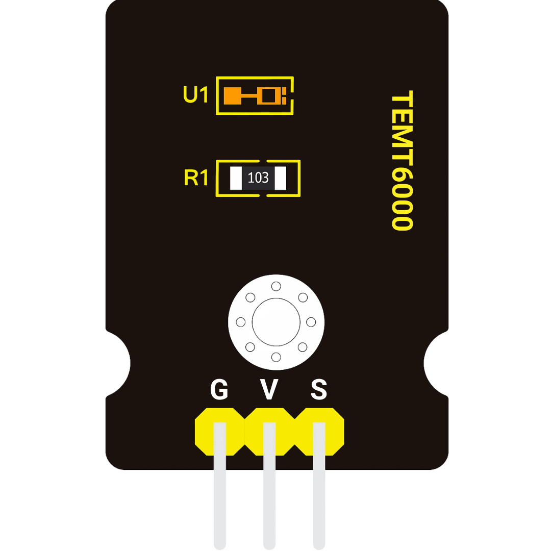
 Design with KS0098 in Cirkit Designer
Introduction
The KS0098 is a versatile integrated circuit (IC) designed for a wide range of applications, including signal processing, control systems, and general-purpose electronic projects. Its robust design and multiple input/output pins make it an ideal choice for hobbyists and professionals alike. The KS0098 is known for its ease of integration, reliability, and adaptability in various circuit designs.
Explore Projects Built with KS0098
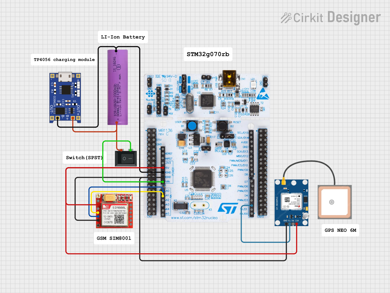
 Open Project in Cirkit Designer
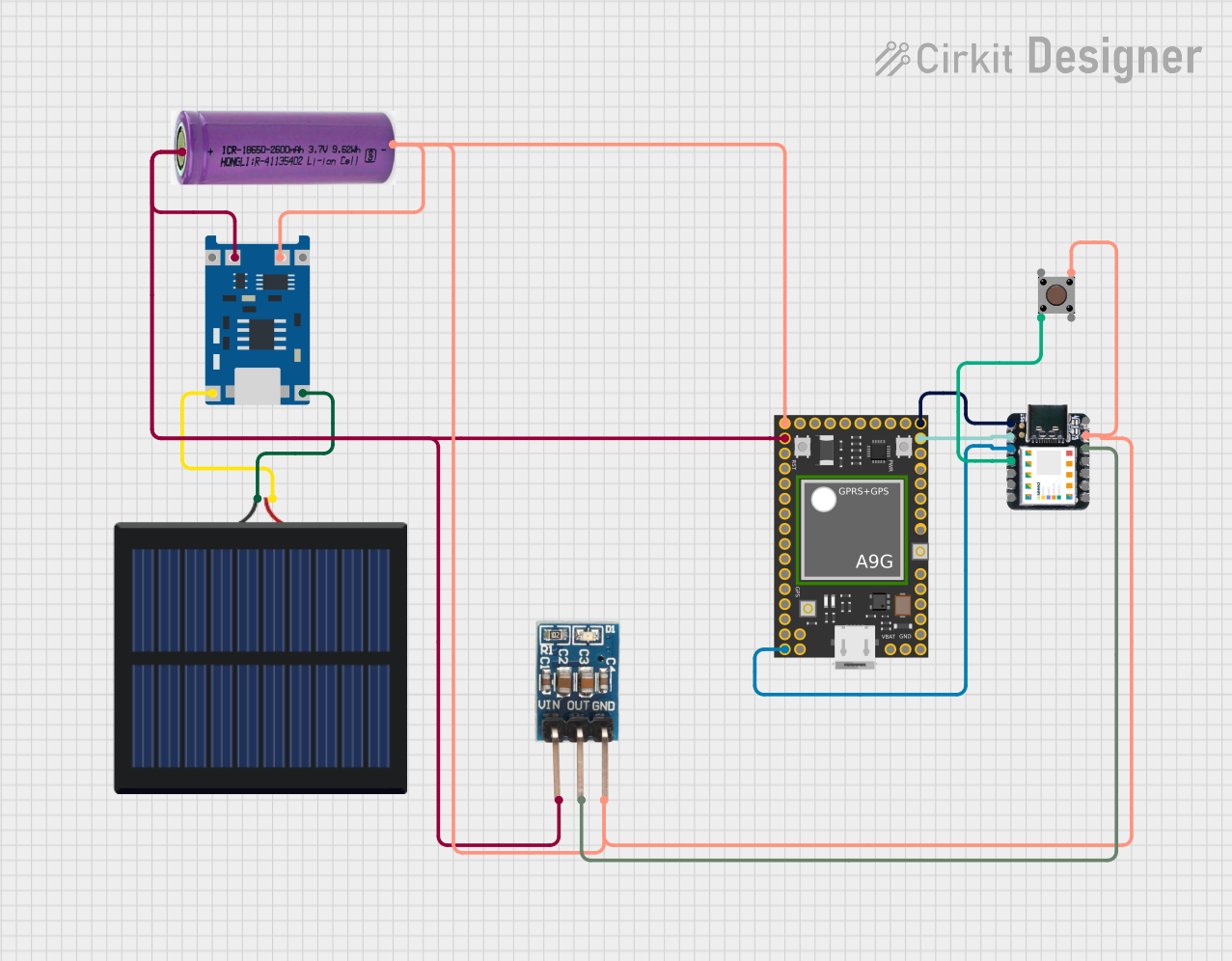
 Open Project in Cirkit Designer
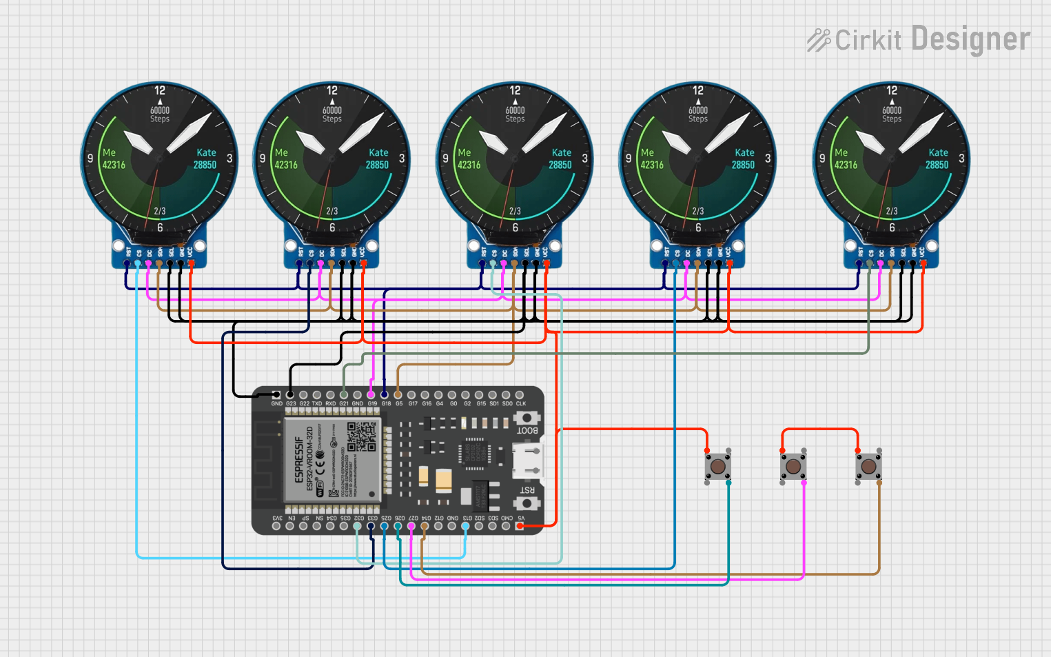
 Open Project in Cirkit Designer
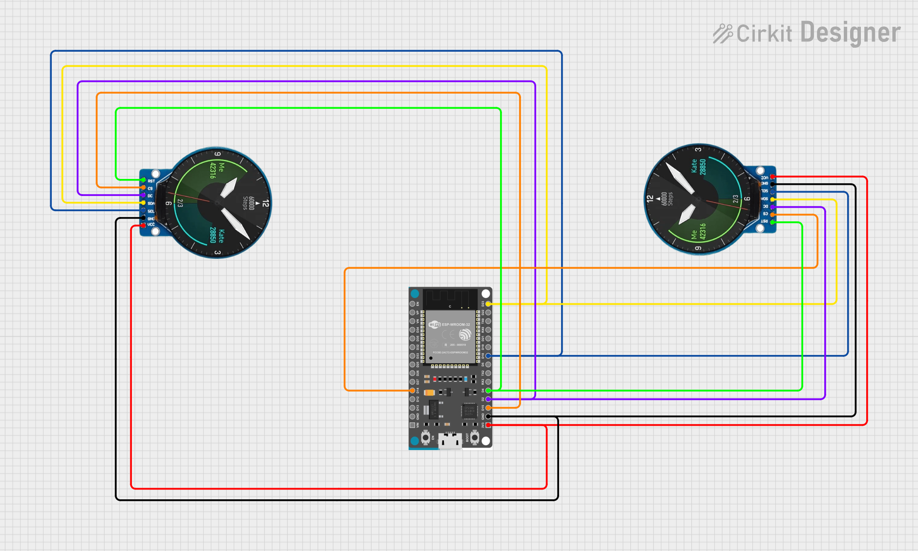
 Open Project in Cirkit Designer
Explore Projects Built with KS0098

 Open Project in Cirkit Designer
 Open Project in Cirkit Designer
 Open Project in Cirkit Designer
 Open Project in Cirkit Designer
Common Applications
- Signal processing in audio and communication systems
- Control systems for automation and robotics
- General-purpose logic and switching circuits
- Prototyping and educational projects
Technical Specifications
The KS0098 is built to handle a variety of tasks with its flexible design. Below are the key technical details:
Key Specifications
- Operating Voltage: 3.3V to 5V
- Maximum Current (per pin): 20mA
- Power Dissipation: 500mW (maximum)
- Operating Temperature Range: -40°C to +85°C
- Input Impedance: 10kΩ (typical)
- Output Impedance: 50Ω (typical)
- Package Type: DIP-16 (Dual Inline Package with 16 pins)
Pin Configuration and Descriptions
The KS0098 features a 16-pin configuration. Below is the pinout and description:
| Pin Number | Pin Name | Description |
|---|---|---|
| 1 | VCC | Power supply input (3.3V to 5V) |
| 2 | GND | Ground connection |
| 3 | IN1 | Input signal 1 |
| 4 | IN2 | Input signal 2 |
| 5 | IN3 | Input signal 3 |
| 6 | IN4 | Input signal 4 |
| 7 | OUT1 | Output signal 1 |
| 8 | OUT2 | Output signal 2 |
| 9 | OUT3 | Output signal 3 |
| 10 | OUT4 | Output signal 4 |
| 11 | ENABLE | Enable pin for activating the IC |
| 12 | RESET | Reset pin for initializing the IC |
| 13 | CLK | Clock input for timing control |
| 14 | DATA | Data input/output for communication |
| 15 | TEST | Test pin for debugging purposes |
| 16 | NC | Not connected (reserved for future use) |
Usage Instructions
The KS0098 is straightforward to use in a variety of circuits. Below are the steps and best practices for integrating it into your project.
How to Use the KS0098
- Power Supply: Connect the VCC pin to a stable 3.3V or 5V power source and the GND pin to the ground of your circuit.
- Input Signals: Connect your input signals to the IN1–IN4 pins. Ensure the input voltage levels are within the operating range of the IC.
- Output Signals: The processed signals will be available at the OUT1–OUT4 pins. Connect these to the desired output devices or circuits.
- Enable the IC: Use the ENABLE pin to activate the IC. Pull it high (logic 1) to enable the IC or low (logic 0) to disable it.
- Reset Function: If needed, use the RESET pin to initialize the IC. Pull it low momentarily to reset the internal state.
- Clock and Data: For applications requiring timing or communication, connect the CLK and DATA pins to the appropriate sources.
Important Considerations
- Decoupling Capacitors: Place a 0.1µF ceramic capacitor close to the VCC and GND pins to filter out noise.
- Input Protection: Use resistors or diodes to protect the input pins from voltage spikes.
- Thermal Management: Ensure adequate ventilation or heat sinking if the IC operates near its maximum power dissipation.
Example: Using KS0098 with Arduino UNO
The KS0098 can be easily interfaced with an Arduino UNO for control and signal processing. Below is an example code snippet:
// Example: Controlling KS0098 with Arduino UNO
// This code demonstrates how to send signals to the KS0098 and read outputs.

#define ENABLE_PIN 7  // Pin connected to KS0098 ENABLE
#define RESET_PIN 8   // Pin connected to KS0098 RESET
#define IN1_PIN 9     // Pin connected to KS0098 IN1
#define OUT1_PIN 10   // Pin connected to KS0098 OUT1

void setup() {
  pinMode(ENABLE_PIN, OUTPUT); // Set ENABLE pin as output
  pinMode(RESET_PIN, OUTPUT);  // Set RESET pin as output
  pinMode(IN1_PIN, OUTPUT);    // Set IN1 pin as output
  pinMode(OUT1_PIN, INPUT);    // Set OUT1 pin as input

  digitalWrite(ENABLE_PIN, HIGH); // Enable the KS0098
  digitalWrite(RESET_PIN, LOW);   // Reset the KS0098
  delay(10);                      // Wait for reset to complete
  digitalWrite(RESET_PIN, HIGH);  // Release reset
}

void loop() {
  digitalWrite(IN1_PIN, HIGH); // Send a HIGH signal to IN1
  delay(1000);                 // Wait for 1 second
  digitalWrite(IN1_PIN, LOW);  // Send a LOW signal to IN1
  delay(1000);                 // Wait for 1 second

  int output = digitalRead(OUT1_PIN); // Read the output from OUT1
  if (output == HIGH) {
    // Perform an action if OUT1 is HIGH
  }
}
Troubleshooting and FAQs
Common Issues
No Output Signal:
- Ensure the ENABLE pin is pulled high to activate the IC.
- Verify that the input signals are within the specified voltage range.
- Check the connections to the output pins.
Overheating:
- Confirm that the IC is not exceeding its maximum power dissipation.
- Use a heat sink or improve ventilation if necessary.
Unstable Operation:
- Add decoupling capacitors near the power pins to reduce noise.
- Verify that the clock and data signals are stable and within specifications.
FAQs
Q1: Can the KS0098 operate at 12V?
A1: No, the KS0098 is designed to operate within a voltage range of 3.3V to 5V. Exceeding this range may damage the IC.
Q2: What is the purpose of the TEST pin?
A2: The TEST pin is reserved for debugging and factory testing. It is not typically used in standard applications.
Q3: How do I protect the IC from voltage spikes?
A3: Use series resistors or clamping diodes on the input pins to prevent voltage spikes from damaging the IC.
By following this documentation, you can effectively integrate and troubleshoot the KS0098 in your electronic projects.