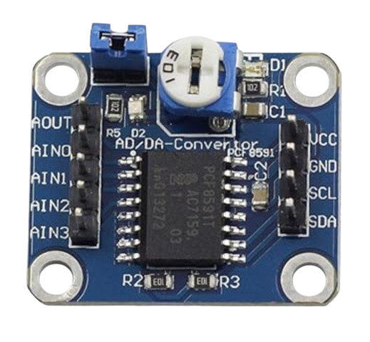
How to Use ADDA: Examples, Pinouts, and Specs
Introduction
An Analog-to-Digital and Digital-to-Analog converter (ADDA) is a versatile electronic component that bridges the gap between analog signals and digital systems. It performs two critical functions: converting analog signals into digital data (ADC) and converting digital data back into analog signals (DAC). This dual functionality makes the ADDA an essential component in modern electronics, enabling seamless communication between analog devices (e.g., sensors, audio equipment) and digital systems (e.g., microcontrollers, computers).
Explore Projects Built with ADDA

Explore Projects Built with ADDA
Common Applications and Use Cases
- Audio Processing: Converting analog audio signals to digital for processing and vice versa for playback.
- Sensor Interfacing: Reading analog sensor data and converting it into digital signals for microcontroller processing.
- Signal Reconstruction: Reconstructing analog signals from digital data in communication systems.
- Data Acquisition Systems: Capturing and processing real-world analog signals for analysis.
- Control Systems: Enabling feedback loops by converting signals between analog and digital domains.
Technical Specifications
Below are the general technical specifications for a typical ADDA module. Specific values may vary depending on the manufacturer and model.
Key Technical Details
- Supply Voltage: 3.3V to 5V
- Input Voltage Range (ADC): 0V to Vref (reference voltage, typically 3.3V or 5V)
- Output Voltage Range (DAC): 0V to Vref
- Resolution: 8-bit, 10-bit, 12-bit, or higher (depending on the model)
- Sampling Rate (ADC): Up to 1 MSPS (Million Samples Per Second)
- Output Settling Time (DAC): Typically in the microsecond range
- Communication Protocols: SPI, I2C, or parallel interface
- Operating Temperature: -40°C to +85°C
Pin Configuration and Descriptions
The pinout of an ADDA module may vary, but a typical configuration is shown below:
| Pin Name | Description |
|---|---|
| VCC | Power supply input (3.3V or 5V). |
| GND | Ground connection. |
| Vref | Reference voltage input for ADC and DAC operations. |
| ADC_IN | Analog input pin for the ADC. |
| DAC_OUT | Analog output pin for the DAC. |
| SCL/CLK | Serial clock input for communication (I2C or SPI). |
| SDA/MOSI | Data line for communication (I2C or SPI). |
| MISO | Data output line for SPI communication (if applicable). |
| CS/SS | Chip select or slave select pin for SPI communication. |
| INT/DRDY | Interrupt or data ready pin (optional, depending on the model). |
Usage Instructions
How to Use the ADDA in a Circuit
- Power the Module: Connect the VCC pin to a 3.3V or 5V power source and the GND pin to ground.
- Set the Reference Voltage: Provide a stable reference voltage to the Vref pin. This voltage determines the ADC input range and DAC output range.
- Connect the Analog Signal: For ADC operation, connect the analog signal to the ADC_IN pin. For DAC operation, the analog output will be available on the DAC_OUT pin.
- Establish Communication: Use the appropriate communication protocol (SPI or I2C) to interface the ADDA with your microcontroller or digital system.
- Write Code: Program your microcontroller to send or receive data to/from the ADDA module.
Important Considerations and Best Practices
- Reference Voltage Stability: Ensure the Vref voltage is stable and noise-free for accurate conversions.
- Input Signal Conditioning: Use filters or amplifiers to condition the analog input signal before feeding it to the ADC.
- Sampling Rate: Choose an appropriate sampling rate for your application to avoid aliasing or data loss.
- Communication Protocol: Match the communication protocol and settings (e.g., clock speed) between the ADDA and your microcontroller.
- Bypass Capacitors: Place bypass capacitors near the VCC and Vref pins to reduce noise and improve performance.
Example: Using ADDA with Arduino UNO
Below is an example of interfacing an ADDA module with an Arduino UNO using SPI communication.
#include <SPI.h>

// Define SPI pins for the ADDA module
const int CS_PIN = 10; // Chip Select pin for SPI communication

void setup() {
  // Initialize SPI communication
  SPI.begin();
  pinMode(CS_PIN, OUTPUT);
  digitalWrite(CS_PIN, HIGH); // Set CS pin to HIGH (inactive)

  Serial.begin(9600); // Initialize serial communication for debugging
}

void loop() {
  // Example: Sending a digital value to the DAC
  uint16_t digitalValue = 512; // 10-bit value (0-1023 for 5V range)

  digitalWrite(CS_PIN, LOW); // Activate the ADDA module
  SPI.transfer16(digitalValue); // Send the 10-bit digital value
  digitalWrite(CS_PIN, HIGH); // Deactivate the ADDA module

  delay(1000); // Wait for 1 second

  // Example: Reading an analog value from the ADC
  digitalWrite(CS_PIN, LOW); // Activate the ADDA module
  uint16_t analogValue = SPI.transfer16(0x0000); // Read 10-bit ADC value
  digitalWrite(CS_PIN, HIGH); // Deactivate the ADDA module

  Serial.print("Analog Value: ");
  Serial.println(analogValue); // Print the ADC value to the serial monitor

  delay(1000); // Wait for 1 second
}
Troubleshooting and FAQs
Common Issues and Solutions
No Output from DAC:
- Cause: Incorrect reference voltage or communication settings.
- Solution: Verify the Vref voltage and ensure the communication protocol is configured correctly.
Inaccurate ADC Readings:
- Cause: Noise in the input signal or unstable reference voltage.
- Solution: Use proper signal conditioning (e.g., filters) and ensure a stable Vref.
Communication Failure:
- Cause: Incorrect wiring or mismatched protocol settings.
- Solution: Double-check the wiring and ensure the SPI/I2C settings (e.g., clock speed) match between the ADDA and microcontroller.
Overheating:
- Cause: Exceeding the voltage or current ratings.
- Solution: Ensure the input voltage and current are within the specified limits.
FAQs
Q: Can I use the ADDA with a 3.3V microcontroller?
- A: Yes, as long as the ADDA module supports 3.3V operation and the reference voltage is set accordingly.
Q: What resolution should I choose for my application?
- A: Higher resolution (e.g., 12-bit) provides more precise conversions but may require more processing power. Choose based on your application's accuracy requirements.
Q: How do I prevent aliasing in ADC applications?
- A: Use an anti-aliasing filter to remove high-frequency components from the input signal before sampling.
Q: Can I use the ADC and DAC simultaneously?
- A: Yes, most ADDA modules support simultaneous ADC and DAC operations, but check the datasheet for specific details.