
How to Use SN74AHCT125N : Examples, Pinouts, and Specs
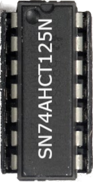
 Design with SN74AHCT125N in Cirkit Designer
Introduction
The SN74AHCT125N, manufactured by Texas Instruments, is a quad buffer/driver with 3-state outputs. This component is designed for high-speed operation and low power consumption, making it ideal for modern digital circuits. Each of the four independent buffers features a 3-state output, which can be controlled via an enable pin. The device operates with TTL-compatible inputs and is commonly used for signal buffering, level shifting, and bus driving in microcontroller and digital logic applications.
Explore Projects Built with SN74AHCT125N
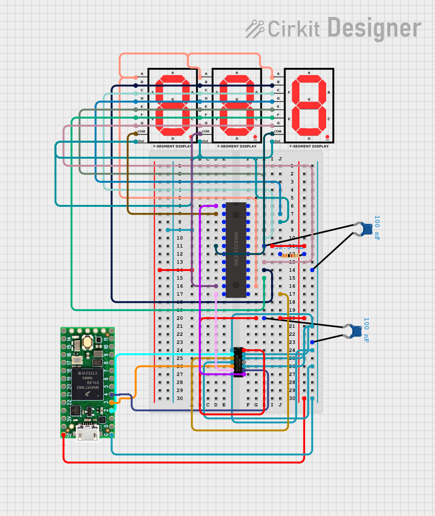 Open Project in Cirkit Designer
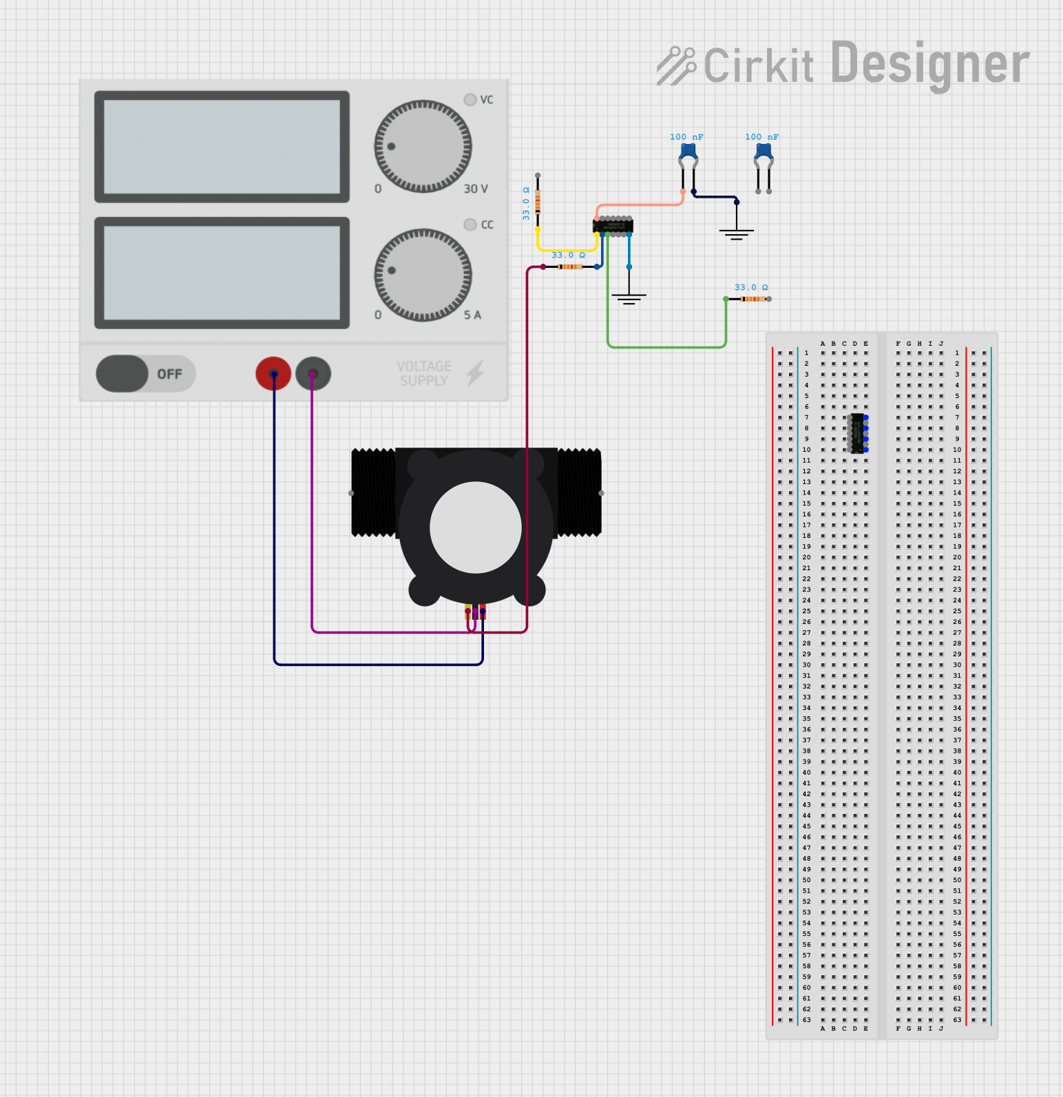 Open Project in Cirkit Designer
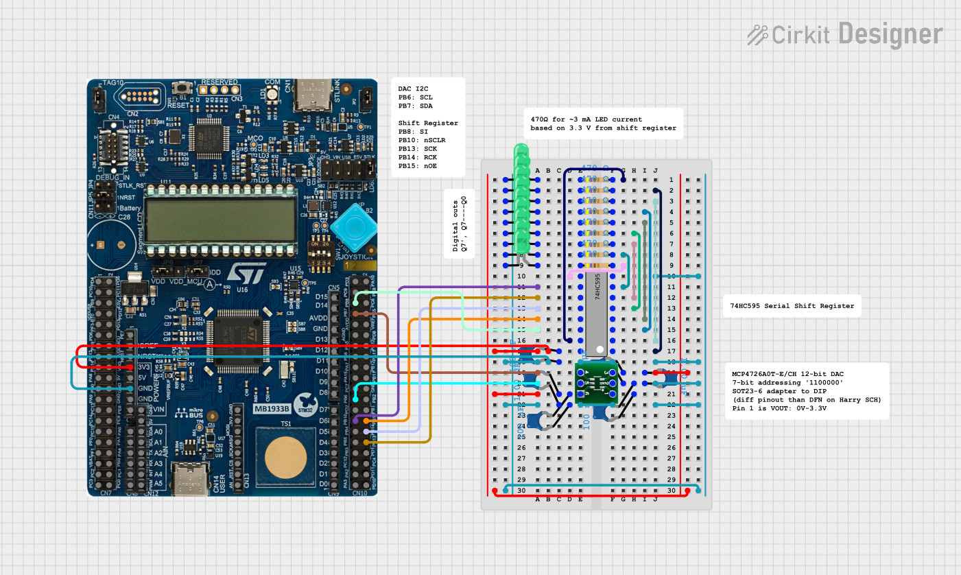 Open Project in Cirkit Designer
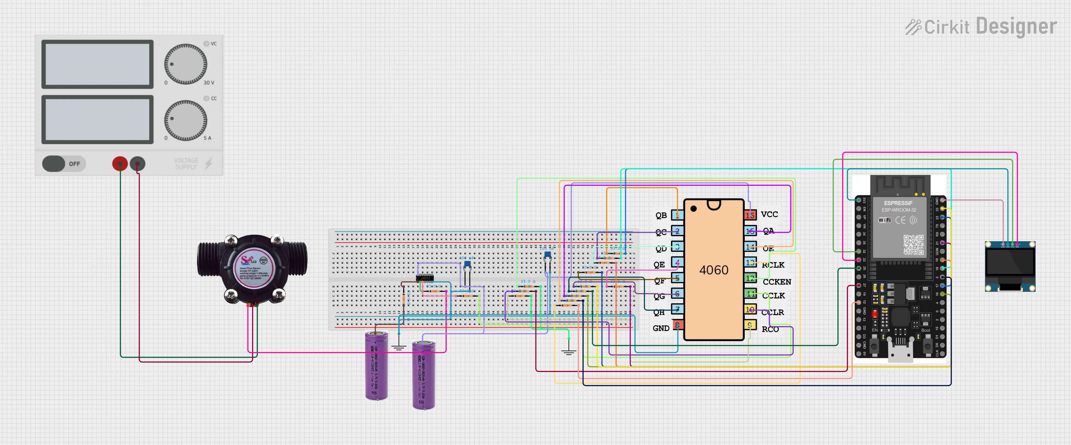 Open Project in Cirkit Designer
Explore Projects Built with SN74AHCT125N
Open Project in Cirkit DesignerOpen Project in Cirkit DesignerOpen Project in Cirkit DesignerOpen Project in Cirkit DesignerCommon Applications
- Signal buffering in digital circuits
- Level shifting between different voltage domains
- Driving data buses in microcontroller systems
- Reducing signal noise and improving signal integrity
- Interfacing between TTL and CMOS logic levels
Technical Specifications
Key Technical Details
| Parameter | Value |
|---|---|
| Supply Voltage (Vcc) | 4.5V to 5.5V |
| Input Voltage Range | 0V to 5.5V |
| High-Level Output Voltage | 4.4V (min) at Vcc = 5V, Iout = -8mA |
| Low-Level Output Voltage | 0.1V (max) at Vcc = 5V, Iout = 8mA |
| Output Current (Iout) | ±25mA |
| Maximum Propagation Delay | 7ns (typical) at Vcc = 5V |
| Operating Temperature Range | -40°C to 85°C |
| Package Type | PDIP-14 |
Pin Configuration and Descriptions
The SN74AHCT125N is housed in a 14-pin PDIP package. The pinout and descriptions are as follows:
| Pin Number | Pin Name | Description |
|---|---|---|
| 1 | 1OE | Output Enable for Buffer 1 (Active Low) |
| 2 | 1A | Input for Buffer 1 |
| 3 | 1Y | Output for Buffer 1 |
| 4 | 2OE | Output Enable for Buffer 2 (Active Low) |
| 5 | 2A | Input for Buffer 2 |
| 6 | 2Y | Output for Buffer 2 |
| 7 | GND | Ground |
| 8 | 3Y | Output for Buffer 3 |
| 9 | 3A | Input for Buffer 3 |
| 10 | 3OE | Output Enable for Buffer 3 (Active Low) |
| 11 | 4Y | Output for Buffer 4 |
| 12 | 4A | Input for Buffer 4 |
| 13 | 4OE | Output Enable for Buffer 4 (Active Low) |
| 14 | Vcc | Positive Supply Voltage |
Usage Instructions
How to Use the SN74AHCT125N in a Circuit
- Power Supply: Connect the Vcc pin (Pin 14) to a 5V power supply and the GND pin (Pin 7) to ground.
- Input Signals: Apply the input signals to the
Apins (Pins 2, 5, 9, and 12) of the respective buffers. - Output Enable: Control the output enable pins (
OE, Pins 1, 4, 10, and 13) to enable or disable the corresponding outputs. When theOEpin is LOW, the output is active. When theOEpin is HIGH, the output is in a high-impedance (3-state) mode. - Outputs: The buffered signals will appear on the
Ypins (Pins 3, 6, 8, and 11) when the correspondingOEpin is LOW.
Important Considerations
- Ensure that the supply voltage (Vcc) is within the specified range of 4.5V to 5.5V.
- Avoid exceeding the maximum output current of ±25mA per pin to prevent damage.
- Use pull-up or pull-down resistors on the
OEpins if they are not actively driven to avoid floating states. - For high-speed applications, minimize trace lengths and use proper decoupling capacitors (e.g., 0.1µF) near the Vcc pin to reduce noise.
Example: Connecting to an Arduino UNO
The SN74AHCT125N can be used with an Arduino UNO to buffer signals or interface with other devices. Below is an example of how to use the component to buffer a digital signal:
Circuit Connections
- Connect the Vcc pin (Pin 14) to the Arduino's 5V pin.
- Connect the GND pin (Pin 7) to the Arduino's GND pin.
- Connect an Arduino digital output pin (e.g., Pin 2) to the
1Apin (Pin 2) of the SN74AHCT125N. - Connect the
1OEpin (Pin 1) to GND to enable the output. - Connect the
1Ypin (Pin 3) to the input of the device you want to drive.
Arduino Code
// Example code to toggle a signal through the SN74AHCT125N buffer

const int bufferInputPin = 2;  // Arduino pin connected to 1A (Pin 2 of SN74AHCT125N)
const int ledPin = 13;         // Built-in LED for visual feedback

void setup() {
  pinMode(bufferInputPin, OUTPUT); // Set buffer input pin as output
  pinMode(ledPin, OUTPUT);         // Set LED pin as output
}

void loop() {
  digitalWrite(bufferInputPin, HIGH); // Send HIGH signal to buffer input
  digitalWrite(ledPin, HIGH);         // Turn on LED
  delay(500);                         // Wait for 500ms

  digitalWrite(bufferInputPin, LOW);  // Send LOW signal to buffer input
  digitalWrite(ledPin, LOW);          // Turn off LED
  delay(500);                         // Wait for 500ms
}
Troubleshooting and FAQs
Common Issues and Solutions
No Output Signal:
- Ensure the
OEpin for the corresponding buffer is connected to GND (active LOW). - Verify that the input signal is within the specified voltage range (0V to 5.5V).
- Ensure the
Output Signal is Distorted:
- Check for proper decoupling capacitors near the Vcc pin to reduce noise.
- Ensure that the output load does not exceed the maximum current rating of ±25mA.
High-Impedance Output When Not Expected:
- Verify that the
OEpin is not floating. Use a pull-down resistor if necessary.
- Verify that the
Device Overheating:
- Ensure that the total current drawn by all outputs does not exceed the maximum power dissipation of the device.
- Check for short circuits on the output pins.
FAQs
Q: Can the SN74AHCT125N be used for level shifting?
A: Yes, the SN74AHCT125N can be used to shift signals from TTL levels to CMOS levels, provided the supply voltage is 5V.
Q: What happens if the OE pin is left floating?
A: A floating OE pin can cause unpredictable behavior. It is recommended to tie the OE pin to GND (active LOW) or use a pull-down resistor.
Q: Can this component drive LEDs directly?
A: While the SN74AHCT125N can source or sink up to ±25mA, it is better to use a current-limiting resistor in series with the LED to prevent damage to the device.