How to Use X-OR Gate: Examples, Pinouts, and Specs
Introduction
- An exclusive OR (X-OR) gate is a digital logic gate that outputs true (logic high) only when the number of true inputs is odd. For a two-input X-OR gate, the output is high when one input is high, and the other is low.
- Common applications of X-OR gates include:
- Arithmetic circuits (e.g., adders and subtractors)
- Digital signal processing
- Parity checking and generation
- Data comparison circuits
- Controlled inverters in multiplexers and demultiplexers
Explore Projects Built with X-OR Gate
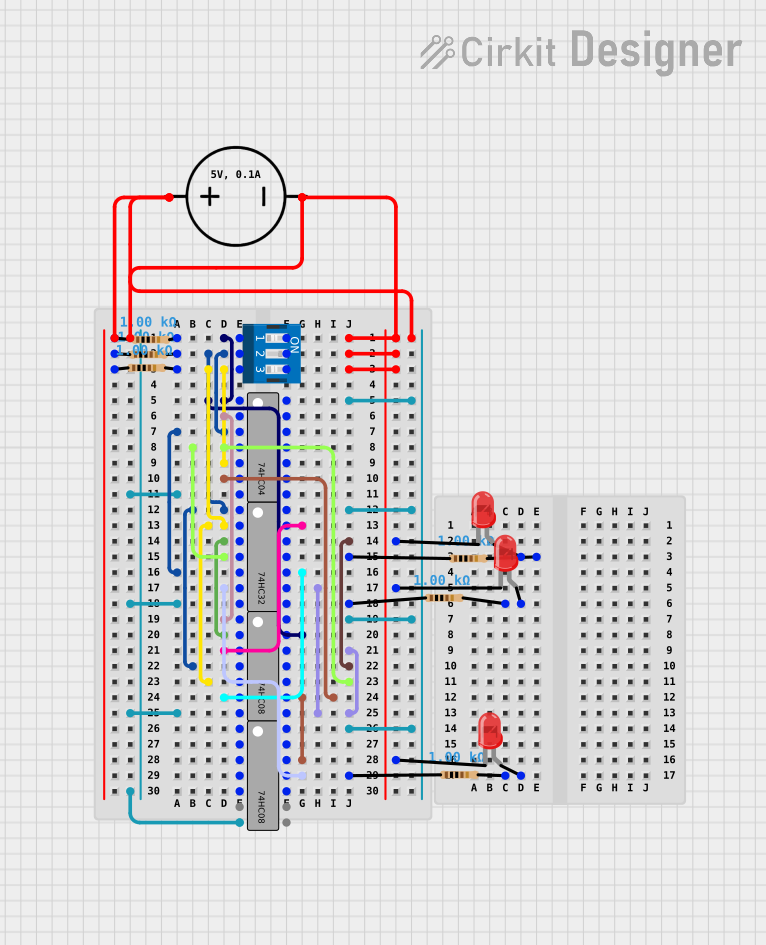
Explore Projects Built with X-OR Gate
Technical Specifications
- Logic Function: ( Y = A \oplus B ), where ( Y ) is the output, and ( A ) and ( B ) are the inputs.
- Voltage Levels:
- Logic Low (0): 0V to 0.8V (typical for TTL logic)
- Logic High (1): 2V to 5V (typical for TTL logic)
- Power Supply: 5V DC (for standard TTL ICs like 74LS86)
- Propagation Delay: ~10ns to 20ns (varies by IC family)
- Power Consumption: ~2mW to 10mW (varies by IC family)
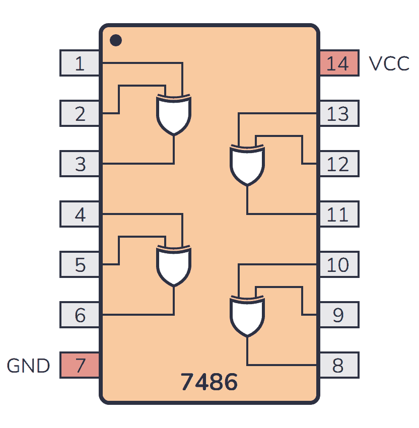
Pin Configuration and Descriptions
Below is the pin configuration for the 74LS86 IC, a commonly used quad 2-input X-OR gate IC:
| Pin Number | Pin Name | Description |
|---|---|---|
| 1 | 1A | Input A for Gate 1 |
| 2 | 1B | Input B for Gate 1 |
| 3 | 1Y | Output of Gate 1 |
| 4 | 2A | Input A for Gate 2 |
| 5 | 2B | Input B for Gate 2 |
| 6 | 2Y | Output of Gate 2 |
| 7 | GND | Ground (0V) |
| 8 | 3Y | Output of Gate 3 |
| 9 | 3A | Input A for Gate 3 |
| 10 | 3B | Input B for Gate 3 |
| 11 | 4Y | Output of Gate 4 |
| 12 | 4A | Input A for Gate 4 |
| 13 | 4B | Input B for Gate 4 |
| 14 | VCC | Positive Power Supply (+5V) |
Usage Instructions
How to Use the X-OR Gate in a Circuit
- Power the IC: Connect the VCC pin (Pin 14) to a +5V DC power supply and the GND pin (Pin 7) to ground.
- Connect Inputs: Provide digital signals (logic high or low) to the input pins (e.g., 1A and 1B for Gate 1).
- Read the Output: The output pin (e.g., 1Y for Gate 1) will provide the result of the X-OR operation.
- Load Considerations: Ensure the output is connected to a load that does not exceed the IC's current driving capability (typically 8mA for TTL logic).
Important Considerations and Best Practices
- Unused Inputs: Tie unused inputs to ground or VCC to avoid floating inputs, which can cause erratic behavior.
- Decoupling Capacitor: Place a 0.1µF ceramic capacitor between VCC and GND near the IC to filter noise.
- Voltage Levels: Ensure input voltage levels are within the specified range for the IC family (e.g., TTL or CMOS).
- Fan-Out: Check the fan-out capability of the IC to ensure it can drive the connected loads.
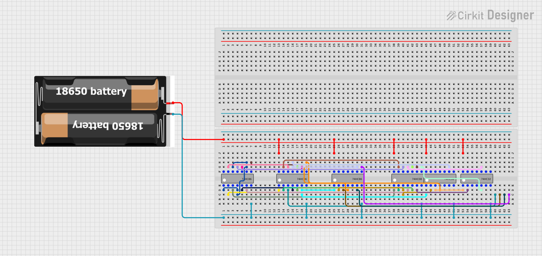
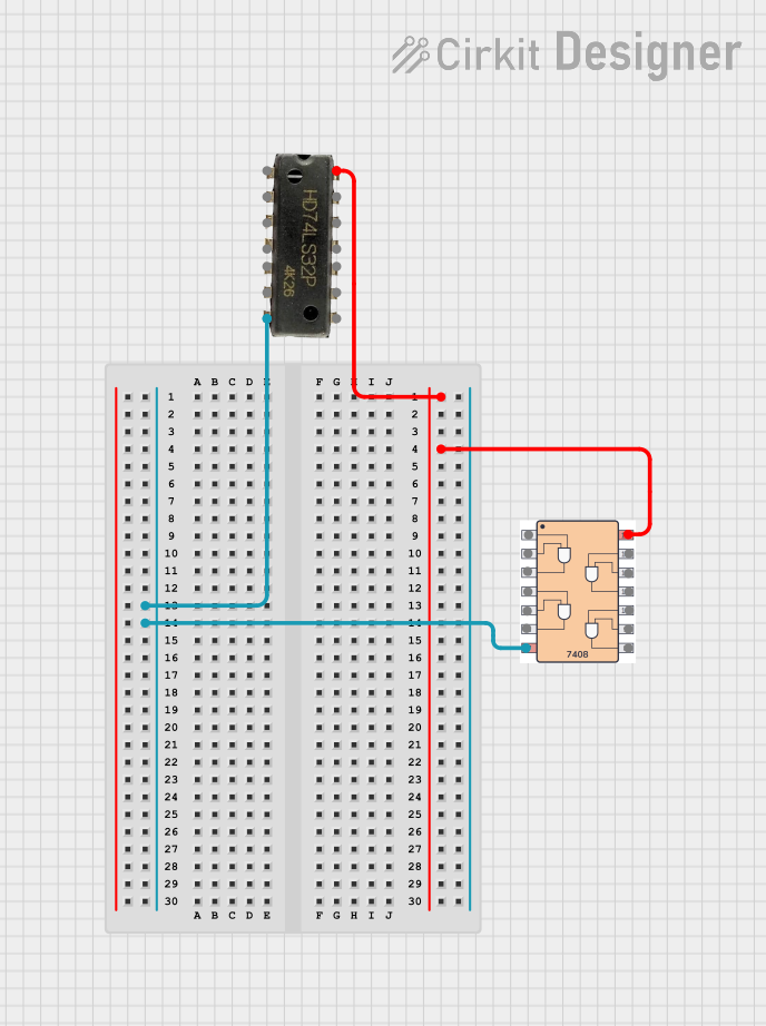
Example: Using an X-OR Gate with Arduino UNO
Below is an example of interfacing a 74LS86 X-OR gate with an Arduino UNO:
Circuit Connections
- Connect Pin 14 (VCC) of the 74LS86 to the Arduino's 5V pin.
- Connect Pin 7 (GND) of the 74LS86 to the Arduino's GND pin.
- Connect Pins 1A and 1B (Pins 1 and 2) to Arduino digital pins 2 and 3, respectively.
- Connect Pin 1Y (Pin 3) to Arduino digital pin 4.
Arduino Code
// Define input pins for the X-OR gate
const int inputA = 2; // Input A connected to Arduino pin 2
const int inputB = 3; // Input B connected to Arduino pin 3

// Define output pin for the X-OR gate
const int outputY = 4; // Output Y connected to Arduino pin 4

void setup() {
  // Set input pins as outputs to drive the X-OR gate
  pinMode(inputA, OUTPUT);
  pinMode(inputB, OUTPUT);

  // Set output pin as input to read the X-OR gate's output
  pinMode(outputY, INPUT);

  // Initialize serial communication for debugging
  Serial.begin(9600);
}

void loop() {
  // Test case: Set input A high and input B low
  digitalWrite(inputA, HIGH);
  digitalWrite(inputB, LOW);

  // Read the output of the X-OR gate
  int xorOutput = digitalRead(outputY);

  // Print the result to the Serial Monitor
  Serial.print("X-OR Output: ");
  Serial.println(xorOutput);

  delay(1000); // Wait for 1 second before the next iteration
}
Troubleshooting and FAQs
Common Issues
No Output Signal:
- Cause: Power supply not connected or incorrect voltage.
- Solution: Verify that VCC and GND are properly connected and the supply voltage is within the IC's range.
Erratic Output:
- Cause: Floating inputs or noise on the power supply.
- Solution: Tie unused inputs to VCC or GND and add a decoupling capacitor near the IC.
Incorrect Logic Levels:
- Cause: Input signals are not within the specified voltage range.
- Solution: Ensure the input signals meet the logic level requirements of the IC.
Overheating:
- Cause: Excessive current draw from the output pins.
- Solution: Check the load connected to the output and ensure it is within the IC's current driving capability.
FAQs
Q: Can I use the X-OR gate with a 3.3V power supply?
A: Standard TTL ICs like the 74LS86 require a 5V supply. For 3.3V operation, use a CMOS variant like the 74HC86.Q: What happens if both inputs are high?
A: The output will be low because the X-OR gate outputs high only when the number of high inputs is odd.Q: Can I cascade multiple X-OR gates?
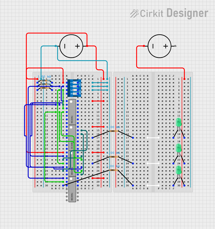
A: Yes, you can cascade X-OR gates to create more complex logic functions, but ensure the output of one gate can drive the input of the next.Q: How do I test the X-OR gate without an Arduino?
A: Use a simple circuit with switches for inputs and an LED for the output. Toggle the switches to observe the X-OR behavior.