How to Use I2C expander: Examples, Pinouts, and Specs
Introduction
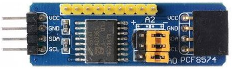
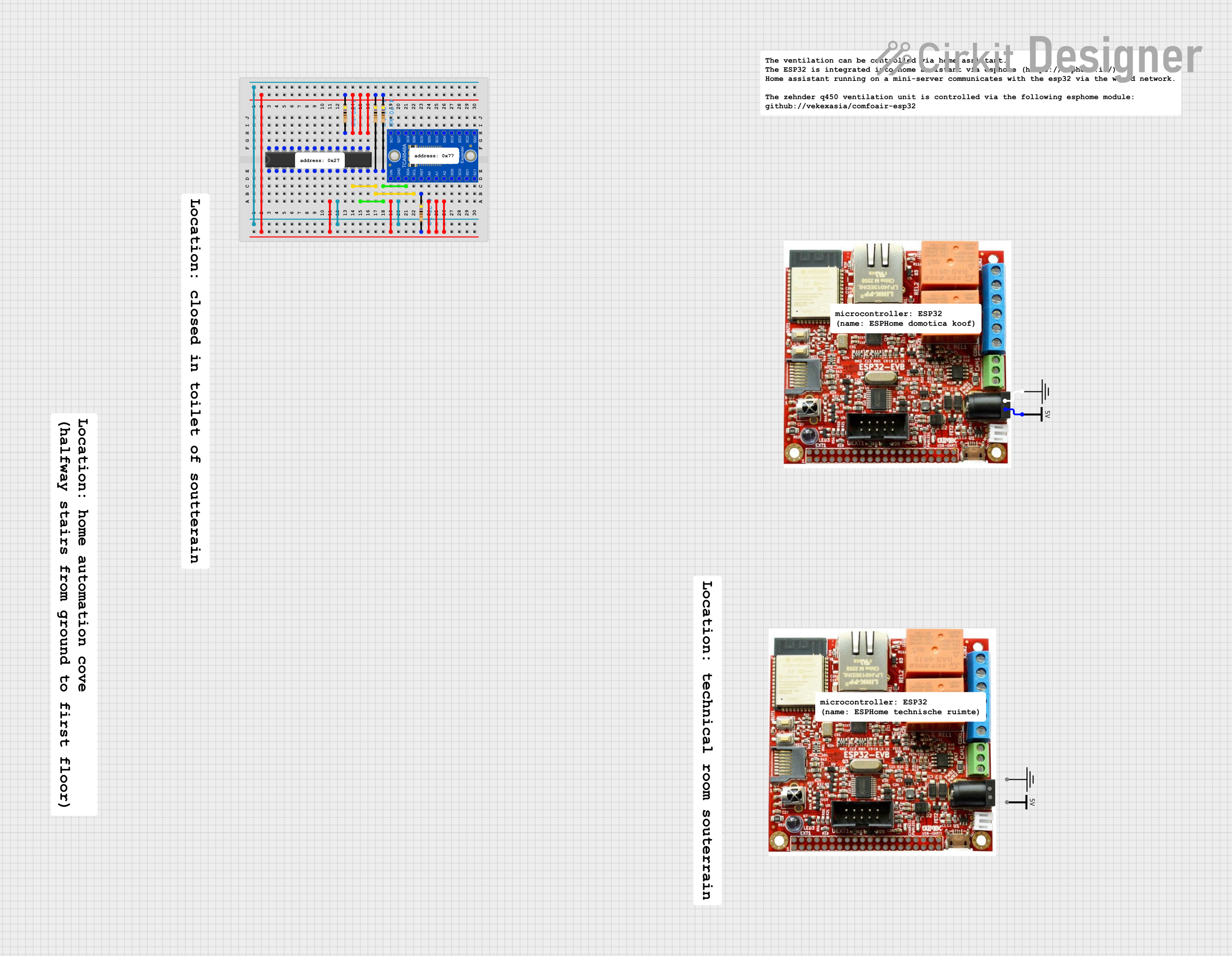
The PCF8574 is an I2C-based I/O expander that allows microcontrollers to interface with additional digital input/output (I/O) pins using the I2C communication protocol. This component is particularly useful when the number of GPIO pins on a microcontroller is insufficient for a given application. By connecting the PCF8574 to the I2C bus, up to 8 additional I/O pins can be added, which can be configured as either inputs or outputs.
Explore Projects Built with I2C expander
Explore Projects Built with I2C expander
Common Applications and Use Cases
- Expanding GPIO pins for microcontrollers like Arduino, Raspberry Pi, or ESP32.
- Driving LEDs, relays, or other digital output devices.
- Reading digital inputs such as switches, buttons, or sensors.
- Building control panels or keypads.
- Interfacing with multiple peripherals in resource-constrained systems.
Technical Specifications
- Manufacturer Part ID: PCF8574
- Communication Protocol: I2C (Inter-Integrated Circuit)
- Operating Voltage: 2.5V to 6V
- Maximum Sink Current (per pin): 25mA
- Maximum Source Current (per pin): -300µA
- I2C Address Range: 0x20 to 0x27 (configurable via address pins A0, A1, A2)
- Number of I/O Pins: 8 (P0 to P7)
- Operating Temperature Range: -40°C to +85°C
- Package Type: DIP, SOIC, or TSSOP (varies by manufacturer)
Pin Configuration and Descriptions
The PCF8574 has 16 pins, with the following configuration:
| Pin Number | Pin Name | Description |
|---|---|---|
| 1 | A0 | Address selection bit 0 (used to set the I2C address) |
| 2 | A1 | Address selection bit 1 (used to set the I2C address) |
| 3 | A2 | Address selection bit 2 (used to set the I2C address) |
| 4 | P0 | General-purpose I/O pin 0 |
| 5 | P1 | General-purpose I/O pin 1 |
| 6 | P2 | General-purpose I/O pin 2 |
| 7 | P3 | General-purpose I/O pin 3 |
| 8 | GND | Ground (0V reference) |
| 9 | P4 | General-purpose I/O pin 4 |
| 10 | P5 | General-purpose I/O pin 5 |
| 11 | P6 | General-purpose I/O pin 6 |
| 12 | P7 | General-purpose I/O pin 7 |
| 13 | INT | Interrupt output (active low, triggered by input pin state changes) |
| 14 | SCL | I2C clock line (connect to microcontroller's SCL pin) |
| 15 | SDA | I2C data line (connect to microcontroller's SDA pin) |
| 16 | VCC | Power supply (2.5V to 6V) |
Usage Instructions
How to Use the PCF8574 in a Circuit
Connect Power and Ground:
- Connect the
VCCpin to the power supply (e.g., 5V for Arduino). - Connect the
GNDpin to the ground of the circuit.
- Connect the
Set the I2C Address:
- Use the
A0,A1, andA2pins to configure the I2C address. These pins can be connected toGND(logic 0) orVCC(logic 1) to set the address. The base address is0x20, and the address can range from0x20to0x27.
- Use the
Connect the I2C Lines:
- Connect the
SCLpin to the microcontroller's I2C clock line. - Connect the
SDApin to the microcontroller's I2C data line. - Use pull-up resistors (typically 4.7kΩ) on the
SCLandSDAlines if not already present.
- Connect the
Connect I/O Devices:
- Use the
P0toP7pins to connect digital input or output devices. Configure these pins in your microcontroller code as needed.
- Use the
Write Code:
- Use an I2C library (e.g., Wire.h for Arduino) to communicate with the PCF8574. Send or receive data to control the I/O pins.
Important Considerations and Best Practices
- Interrupt Pin: The
INTpin can be used to detect changes in input states. This is useful for applications requiring event-driven input handling. - Current Limitations: The PCF8574 can sink up to 25mA per pin but can only source a small current (-300µA). Use external transistors or drivers for high-current applications.
- I2C Pull-Up Resistors: Ensure proper pull-up resistors are present on the I2C lines to maintain signal integrity.
- Address Conflicts: Avoid address conflicts when using multiple I2C devices on the same bus.
Example Code for Arduino UNO
#include <Wire.h> // Include the Wire library for I2C communication

#define PCF8574_ADDRESS 0x20 // Base I2C address of the PCF8574

void setup() {
  Wire.begin(); // Initialize I2C communication
  Serial.begin(9600); // Initialize serial communication for debugging

  // Set all pins (P0 to P7) as outputs and turn them off
  Wire.beginTransmission(PCF8574_ADDRESS);
  Wire.write(0xFF); // Write 0xFF to set all pins high (off for active-low devices)
  Wire.endTransmission();
}

void loop() {
  // Example: Toggle P0 every second
  static bool state = false;
  state = !state;

  Wire.beginTransmission(PCF8574_ADDRESS);
  Wire.write(state ? 0xFE : 0xFF); // Toggle P0 (0xFE = 11111110, 0xFF = 11111111)
  Wire.endTransmission();

  delay(1000); // Wait for 1 second
}
Troubleshooting and FAQs
Common Issues and Solutions
I2C Communication Fails:
- Cause: Incorrect wiring or missing pull-up resistors.
- Solution: Verify connections and ensure 4.7kΩ pull-up resistors are present on the
SCLandSDAlines.
Device Not Responding:
- Cause: Incorrect I2C address configuration.
- Solution: Check the
A0,A1, andA2pin connections and calculate the correct address.
Output Pins Not Driving High Current Devices:
- Cause: PCF8574 has limited current sourcing capability.
- Solution: Use external transistors or drivers for high-current loads.
Interrupt Pin Not Working:
- Cause: Interrupts not enabled or misconfigured.
- Solution: Ensure the
INTpin is connected to a microcontroller interrupt-capable pin and properly configured in the code.
FAQs
Can I use multiple PCF8574 devices on the same I2C bus? Yes, up to 8 devices can be used by configuring unique addresses using the
A0,A1, andA2pins.What happens if I exceed the current limits? Exceeding the current limits can damage the PCF8574 or cause unreliable operation. Always stay within the specified ratings.
Can the PCF8574 handle analog signals? No, the PCF8574 is designed for digital I/O only. Use an ADC (Analog-to-Digital Converter) for analog signals.
Is the PCF8574 compatible with 3.3V systems? Yes, the PCF8574 operates from 2.5V to 6V, making it compatible with both 3.3V and 5V systems.