How to Use 74HC74: Examples, Pinouts, and Specs

Introduction
The 74HC74 is a dual positive-edge triggered D-type flip-flop with individual data, set, reset, and clock inputs; and Q and Q-bar outputs. This integrated circuit (IC) is widely used in digital electronics for storing and processing binary data. It is a fundamental building block in sequential logic circuits, counters, shift registers, and memory storage devices.
Explore Projects Built with 74HC74
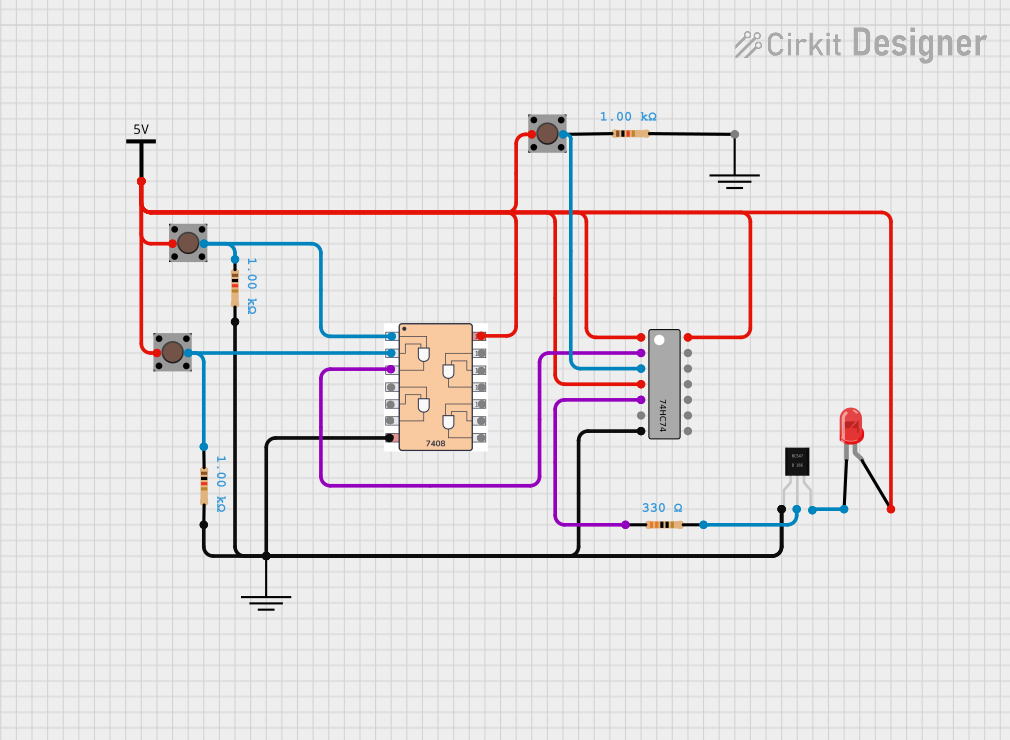
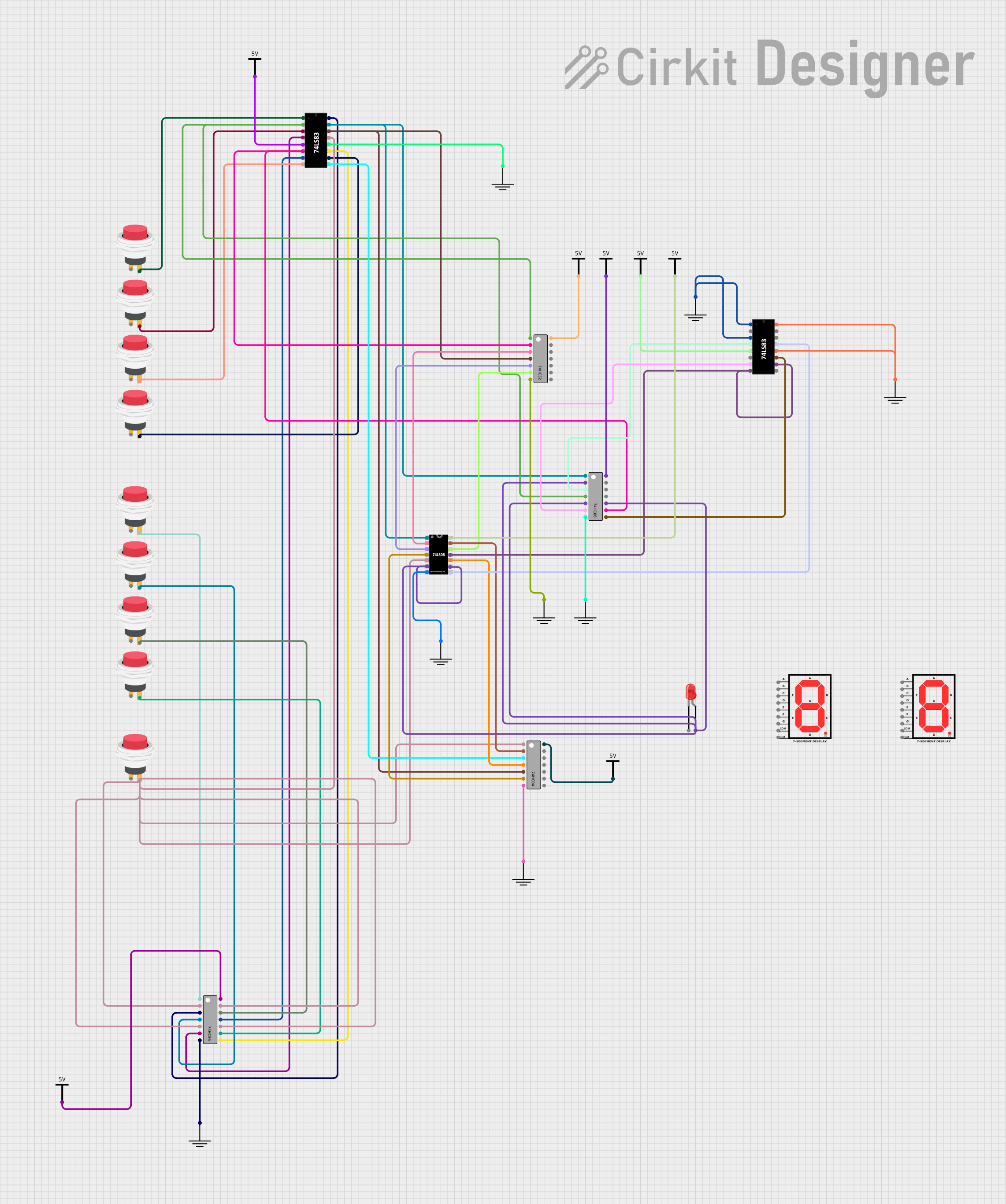
Explore Projects Built with 74HC74
Common Applications and Use Cases
- Digital counters and dividers
- Shift registers
- Data storage
- Synchronous circuits
- Memory registers
- Flip-flop based state machines
Technical Specifications
Key Technical Details
- Logic Family: HC
- Operating Voltage Range: 2V to 6V
- High-Level Input Voltage (V_IH): Minimum 2V
- Low-Level Input Voltage (V_IL): Maximum 0.8V
- High-Level Output Current (I_OH): -5.2 mA (max)
- Low-Level Output Current (I_OL): 5.2 mA (max)
- Propagation Delay Time: Approx. 13 ns (V_CC = 4.5V)
- Setup Time: Approx. 20 ns (V_CC = 4.5V)
- Hold Time: Approx. 5 ns (V_CC = 4.5V)
- Operating Temperature Range: -40°C to +125°C
Pin Configuration and Descriptions
| Pin Number | Name | Description |
|---|---|---|
| 1 | 1CLR | Direct clear input for flip-flop 1 (active low) |
| 2 | 1D | Data input for flip-flop 1 |
| 3 | 1CLK | Clock input for flip-flop 1 (rising edge-triggered) |
| 4 | 1PR | Direct set input for flip-flop 1 (active low) |
| 5 | 1Q | Non-inverted output for flip-flop 1 |
| 6 | 1Q̅ | Inverted output for flip-flop 1 |
| 7 | GND | Ground (0V) |
| 8 | 2Q̅ | Inverted output for flip-flop 2 |
| 9 | 2Q | Non-inverted output for flip-flop 2 |
| 10 | 2PR | Direct set input for flip-flop 2 (active low) |
| 11 | 2CLK | Clock input for flip-flop 2 (rising edge-triggered) |
| 12 | 2D | Data input for flip-flop 2 |
| 13 | 2CLR | Direct clear input for flip-flop 2 (active low) |
| 14 | V_CC | Positive supply voltage |
Usage Instructions
How to Use the 74HC74 in a Circuit
- Power Supply: Connect the V_CC pin to a positive supply voltage within the 2V to 6V range and the GND pin to the ground of the circuit.
- Clock Signal: Apply a clock signal to the CLK input(s) of the flip-flop(s) you wish to use. The flip-flop(s) will trigger on the rising edge of this signal.
- Data Input: Set the desired data bit on the D input(s) that will be stored on the next rising edge of the clock.
- Set/Reset Inputs: Optionally, use the PR (preset) and CLR (clear) inputs to set or reset the flip-flop outputs directly. These are active-low inputs.
- Output: The Q and Q̅ outputs will reflect the stored data bit and its complement, respectively.
Important Considerations and Best Practices
- Ensure that the power supply voltage is within the specified range to prevent damage.
- Avoid floating inputs by connecting unused set/reset inputs to V_CC (inactive state).
- Minimize noise by keeping the clock signal path short and using proper decoupling capacitors near the V_CC pin.
- To prevent unintended state changes, ensure that the setup and hold times for the data inputs are met relative to the clock signal.
Troubleshooting and FAQs
Common Issues Users Might Face
- Unstable Outputs: This can be caused by floating inputs or noise on the clock line. Ensure all inputs are properly connected and that the circuit is well-decoupled.
- Unexpected State Changes: If the flip-flop changes state unexpectedly, check that the setup and hold times for the data inputs are being met.
Solutions and Tips for Troubleshooting
- Floating Inputs: Connect unused inputs to V_CC or GND as appropriate.
- Noise Issues: Use a low-pass filter or a Schmitt trigger buffer on the clock input to reduce noise sensitivity.
- Power Supply Decoupling: Place a 0.1 µF capacitor close to the V_CC pin to filter out noise on the power supply line.
FAQs
Q: Can I use the 74HC74 at 5V? A: Yes, the 74HC74 operates within a range of 2V to 6V, so it is compatible with a 5V supply.
Q: What happens if I don't connect the set or reset pins? A: The set (PR) and reset (CLR) pins are active-low inputs. If left unconnected, they can potentially float to a low level and undesirably set or reset the flip-flop. It is best practice to tie these pins to V_CC if they are not used.
Q: How fast can the 74HC74 operate? A: The maximum operating frequency depends on the supply voltage, but it can typically operate at several megahertz. Check the propagation delay specifications in the datasheet for more precise timing information.
Example Code for Arduino UNO
// Example code to toggle the state of the flip-flop on an Arduino UNO

const int clockPin = 2; // Connect to 1CLK or 2CLK
const int dataPin = 3;   // Connect to 1D or 2D
const int resetPin = 4;  // Connect to 1CLR or 2CLR (active low)

void setup() {
  pinMode(clockPin, OUTPUT);
  pinMode(dataPin, OUTPUT);
  pinMode(resetPin, OUTPUT);

  // Reset the flip-flop at the start
  digitalWrite(resetPin, LOW);
  delay(10);
  digitalWrite(resetPin, HIGH);
}

void loop() {
  // Set data to HIGH
  digitalWrite(dataPin, HIGH);
  // Toggle the clock to store the data
  digitalWrite(clockPin, HIGH);
  delay(10); // Wait for more than the setup time
  digitalWrite(clockPin, LOW);

  // Set data to LOW
  digitalWrite(dataPin, LOW);
  // Toggle the clock to store the data
  digitalWrite(clockPin, HIGH);
  delay(10); // Wait for more than the setup time
  digitalWrite(clockPin, LOW);

  delay(1000); // Wait for 1 second
}
This code demonstrates how to toggle the state of the flip-flop using an Arduino UNO. The flip-flop stores the value present on the data pin at the rising edge of the clock signal. The reset pin is used to clear the flip-flop at the beginning of the program. Ensure that the 74HC74's V_CC and GND pins are connected to the Arduino's 5V and GND, respectively.