Cirkit Designer Logo
Cirkit Designer
Your all-in-one circuit design IDE
Home / 
Component Documentation

How to Use XC4492: Examples, Pinouts, and Specs

Image of XC4492
Cirkit Designer LogoDesign with XC4492 in Cirkit Designer

Introduction

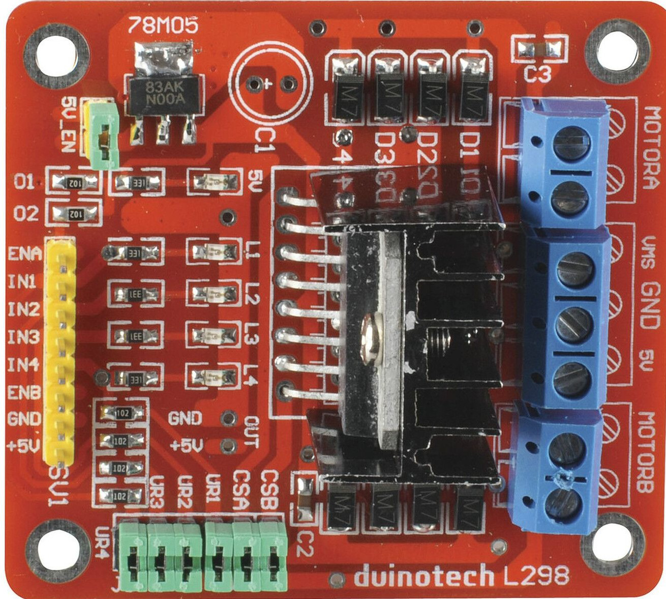
The XC4492, manufactured by DuninoTech, is a high-performance FPGA (Field-Programmable Gate Array) designed for complex digital logic applications. This versatile component allows users to implement custom hardware designs and reprogram the device for various tasks, making it ideal for applications requiring flexibility and scalability. The XC4492 is widely used in industries such as telecommunications, aerospace, automotive, and embedded systems.

Explore Projects Built with XC4492

Use Cirkit Designer to design, explore, and prototype these projects online. Some projects support real-time simulation. Click "Open Project" to start designing instantly!
Satellite-Based Timing and Navigation System with SDR and Atomic Clock Synchronization
Image of GPS 시스템 측정 구성도_Confirm: A project utilizing XC4492 in a practical application
This circuit appears to be a complex system involving power supply management, GPS and timing synchronization, and data communication. It includes a SI-TEX G1 Satellite Compass for GPS data, an XHTF1021 Atomic Rubidium Clock for precise timing, and Ettus USRP B200 units for software-defined radio communication. Power is supplied through various SMPS units and distributed via terminal blocks and DC jacks. Data communication is facilitated by Beelink MINI S12 N95 computers, RS232 splitters, and a 1000BASE-T Media Converter for network connectivity. RF Directional Couplers are used to interface antennas with the USRP units, and the entire system is likely contained within cases for protection and organization.
Cirkit Designer LogoOpen Project in Cirkit Designer
Cellular-Enabled IoT Device with Real-Time Clock and Power Management
Image of LRCM PHASE 2 BASIC: A project utilizing XC4492 in a practical application
This circuit features a LilyGo-SIM7000G module for cellular communication and GPS functionality, interfaced with an RTC DS3231 for real-time clock capabilities. It includes voltage sensing through two voltage sensor modules, and uses an 8-channel opto-coupler for isolating different parts of the circuit. Power management is handled by a buck converter connected to a DC power source and batteries, with a fuse for protection and a rocker switch for on/off control. Additionally, there's an LED for indication purposes.
Cirkit Designer LogoOpen Project in Cirkit Designer
Cellular-Connected ESP32-CAM with Real-Time Clock and Isolated Control
Image of LRCM PHASE 2 PRO: A project utilizing XC4492 in a practical application
This circuit integrates a LilyGo-SIM7000G module with an RTC DS3231 for timekeeping, interfaced via I2C (SCL and SDA lines). An 8-Channel OPTO-COUPLER is used to isolate and interface external signals with the LilyGo-SIM7000G's GPIOs. Power is managed by a Buck converter, which steps down voltage from a DC Power Source to supply the ESP32-CAM and LilyGo-SIM7000G modules, as well as the OPTO-COUPLER.
Cirkit Designer LogoOpen Project in Cirkit Designer
Lilygo 7670e-Based Smart Interface with LCD Display and Keypad
Image of Paower: A project utilizing XC4492 in a practical application
This circuit features a Lilygo 7670e microcontroller interfaced with a 16x2 I2C LCD for display, a 4X4 membrane matrix keypad for input, and an arcade button for additional control. It also includes a 4G antenna and a GPS antenna for communication and location tracking capabilities.
Cirkit Designer LogoOpen Project in Cirkit Designer

Explore Projects Built with XC4492

Use Cirkit Designer to design, explore, and prototype these projects online. Some projects support real-time simulation. Click "Open Project" to start designing instantly!
Image of GPS 시스템 측정 구성도_Confirm: A project utilizing XC4492 in a practical application
Satellite-Based Timing and Navigation System with SDR and Atomic Clock Synchronization
This circuit appears to be a complex system involving power supply management, GPS and timing synchronization, and data communication. It includes a SI-TEX G1 Satellite Compass for GPS data, an XHTF1021 Atomic Rubidium Clock for precise timing, and Ettus USRP B200 units for software-defined radio communication. Power is supplied through various SMPS units and distributed via terminal blocks and DC jacks. Data communication is facilitated by Beelink MINI S12 N95 computers, RS232 splitters, and a 1000BASE-T Media Converter for network connectivity. RF Directional Couplers are used to interface antennas with the USRP units, and the entire system is likely contained within cases for protection and organization.
Cirkit Designer LogoOpen Project in Cirkit Designer
Image of LRCM PHASE 2 BASIC: A project utilizing XC4492 in a practical application
Cellular-Enabled IoT Device with Real-Time Clock and Power Management
This circuit features a LilyGo-SIM7000G module for cellular communication and GPS functionality, interfaced with an RTC DS3231 for real-time clock capabilities. It includes voltage sensing through two voltage sensor modules, and uses an 8-channel opto-coupler for isolating different parts of the circuit. Power management is handled by a buck converter connected to a DC power source and batteries, with a fuse for protection and a rocker switch for on/off control. Additionally, there's an LED for indication purposes.
Cirkit Designer LogoOpen Project in Cirkit Designer
Image of LRCM PHASE 2 PRO: A project utilizing XC4492 in a practical application
Cellular-Connected ESP32-CAM with Real-Time Clock and Isolated Control
This circuit integrates a LilyGo-SIM7000G module with an RTC DS3231 for timekeeping, interfaced via I2C (SCL and SDA lines). An 8-Channel OPTO-COUPLER is used to isolate and interface external signals with the LilyGo-SIM7000G's GPIOs. Power is managed by a Buck converter, which steps down voltage from a DC Power Source to supply the ESP32-CAM and LilyGo-SIM7000G modules, as well as the OPTO-COUPLER.
Cirkit Designer LogoOpen Project in Cirkit Designer
Image of Paower: A project utilizing XC4492 in a practical application
Lilygo 7670e-Based Smart Interface with LCD Display and Keypad
This circuit features a Lilygo 7670e microcontroller interfaced with a 16x2 I2C LCD for display, a 4X4 membrane matrix keypad for input, and an arcade button for additional control. It also includes a 4G antenna and a GPS antenna for communication and location tracking capabilities.
Cirkit Designer LogoOpen Project in Cirkit Designer

Common Applications and Use Cases

  • Digital signal processing (DSP)
  • Prototyping custom hardware designs
  • High-speed data acquisition and processing
  • Hardware acceleration for machine learning and AI
  • Communication protocol implementation
  • Embedded system design and development

Technical Specifications

Key Technical Details

  • Manufacturer: DuninoTech
  • Part ID: XC4492
  • Logic Cells: 50,000
  • Block RAM: 2 MB
  • Clock Speed: Up to 400 MHz
  • I/O Pins: 120
  • Operating Voltage: 1.2V core, 3.3V I/O
  • Power Consumption: 5W (typical)
  • Package Type: BGA (Ball Grid Array)
  • Temperature Range: -40°C to +85°C

Pin Configuration and Descriptions

The XC4492 features 120 I/O pins, organized into functional groups. Below is a summary of the pin configuration:

Pin Group Pin Count Description
General I/O 80 Configurable input/output pins for interfacing with external devices.
Power Supply 10 Pins for core (1.2V) and I/O (3.3V) power supply.
Ground 10 Ground pins for stable operation.
Clock Inputs 4 Dedicated pins for external clock signals.
Configuration Pins 6 Pins for programming and configuring the FPGA.
JTAG Interface 5 Pins for debugging and boundary scan testing.
Reserved 5 Reserved for future use or manufacturer-specific functions.

Usage Instructions

How to Use the XC4492 in a Circuit

  1. Power Supply: Ensure the FPGA is powered with a 1.2V core voltage and 3.3V for I/O. Use decoupling capacitors near the power pins to minimize noise.
  2. Clock Signal: Provide a stable clock signal to one of the dedicated clock input pins. The clock frequency should not exceed 400 MHz.
  3. Programming: Use a JTAG programmer or a configuration memory device to load the desired bitstream into the FPGA.
  4. I/O Configuration: Configure the I/O pins as input, output, or bidirectional based on your design requirements. This is done during the design phase using FPGA development tools.
  5. Cooling: For high-performance applications, consider using a heat sink or active cooling to manage heat dissipation.

Important Considerations and Best Practices

  • Design Tools: Use DuninoTech's official FPGA development suite or compatible third-party tools to design and simulate your logic circuits.
  • Signal Integrity: Keep traces short and use proper termination techniques to maintain signal integrity, especially for high-speed signals.
  • Power Management: Monitor power consumption and ensure your power supply can handle the typical 5W load.
  • Reprogramming: The XC4492 can be reprogrammed multiple times, but ensure the bitstream is verified to avoid configuration errors.

Example: Connecting XC4492 to an Arduino UNO

While the XC4492 is a high-performance FPGA, it can interface with microcontrollers like the Arduino UNO for control or data exchange. Below is an example of how to send data from the Arduino to the FPGA:

// Arduino UNO to XC4492 Communication Example
// This example sends a byte of data to the FPGA via digital pins.

const int fpgaDataPin = 7;  // Pin connected to FPGA data input
const int fpgaClockPin = 8; // Pin connected to FPGA clock input

void setup() {
  pinMode(fpgaDataPin, OUTPUT);  // Set data pin as output
  pinMode(fpgaClockPin, OUTPUT); // Set clock pin as output
}

void loop() {
  byte dataToSend = 0xA5; // Example data to send (10100101 in binary)

  for (int i = 7; i >= 0; i--) {
    // Send each bit of the data, starting with the MSB
    digitalWrite(fpgaDataPin, (dataToSend >> i) & 0x01);
    digitalWrite(fpgaClockPin, HIGH); // Generate clock pulse
    delayMicroseconds(10);            // Short delay for clock pulse
    digitalWrite(fpgaClockPin, LOW);
  }

  delay(1000); // Wait 1 second before sending the next byte
}

Troubleshooting and FAQs

Common Issues and Solutions

  1. FPGA Not Powering On

    • Cause: Incorrect power supply voltage or insufficient current.
    • Solution: Verify the power supply provides 1.2V for the core and 3.3V for I/O. Check the current rating of the power supply.
  2. Configuration Fails

    • Cause: Faulty bitstream or incorrect configuration pins setup.
    • Solution: Recheck the bitstream file and ensure the configuration pins are connected properly.
  3. Overheating

    • Cause: High power consumption or inadequate cooling.
    • Solution: Use a heat sink or active cooling. Ensure the FPGA is not overloaded.
  4. Signal Integrity Issues

    • Cause: Long traces or improper termination.
    • Solution: Shorten trace lengths and use proper termination resistors.

FAQs

  • Q: Can the XC4492 be used for AI applications?
    A: Yes, the XC4492 is suitable for AI and machine learning tasks, especially for hardware acceleration.

  • Q: How many times can the FPGA be reprogrammed?
    A: The XC4492 supports virtually unlimited reprogramming cycles, as it uses SRAM-based configuration.

  • Q: What is the maximum clock frequency?
    A: The maximum clock frequency is 400 MHz.

  • Q: Does the XC4492 support external memory?
    A: Yes, the FPGA can interface with external memory modules such as DDR3 or DDR4.

This concludes the documentation for the XC4492 FPGA. For further assistance, refer to DuninoTech's official resources or contact technical support.