How to Use PAD: Examples, Pinouts, and Specs

Introduction
A PAD (Passive Analog Device) is a terminal or connection point on a circuit board designed to facilitate the attachment of components or connections to the circuit. These pads are typically used for soldering electronic components, such as resistors, capacitors, or integrated circuits, onto a printed circuit board (PCB). They come in various shapes and sizes, including circular, rectangular, and oval, depending on the design requirements of the PCB.
Common applications of PADs include:
- Providing soldering points for through-hole or surface-mount components.
- Acting as test points for debugging and troubleshooting circuits.
- Serving as connection points for external wires or connectors.
- Enabling modularity in circuit design by allowing easy replacement of components.
Explore Projects Built with PAD
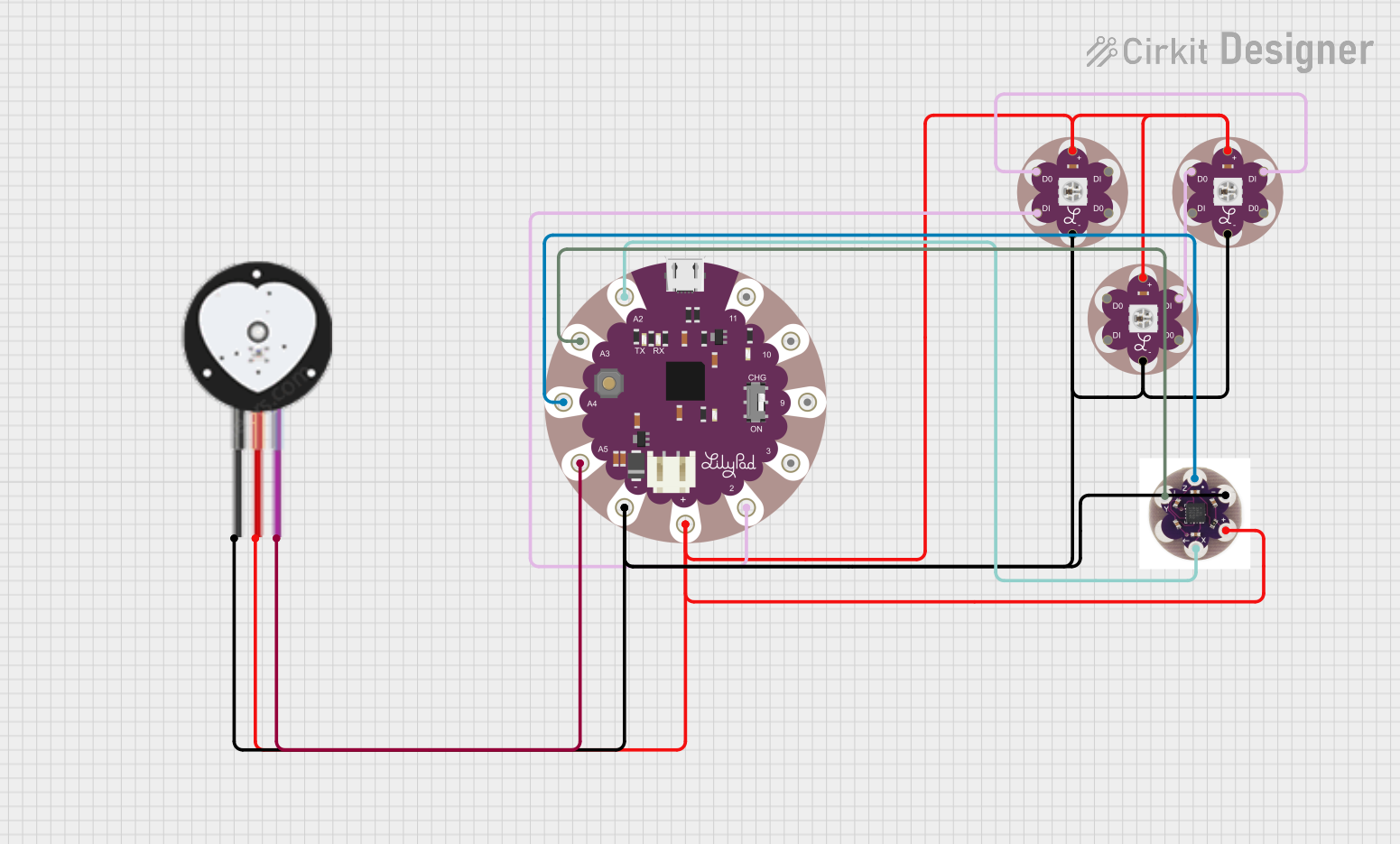
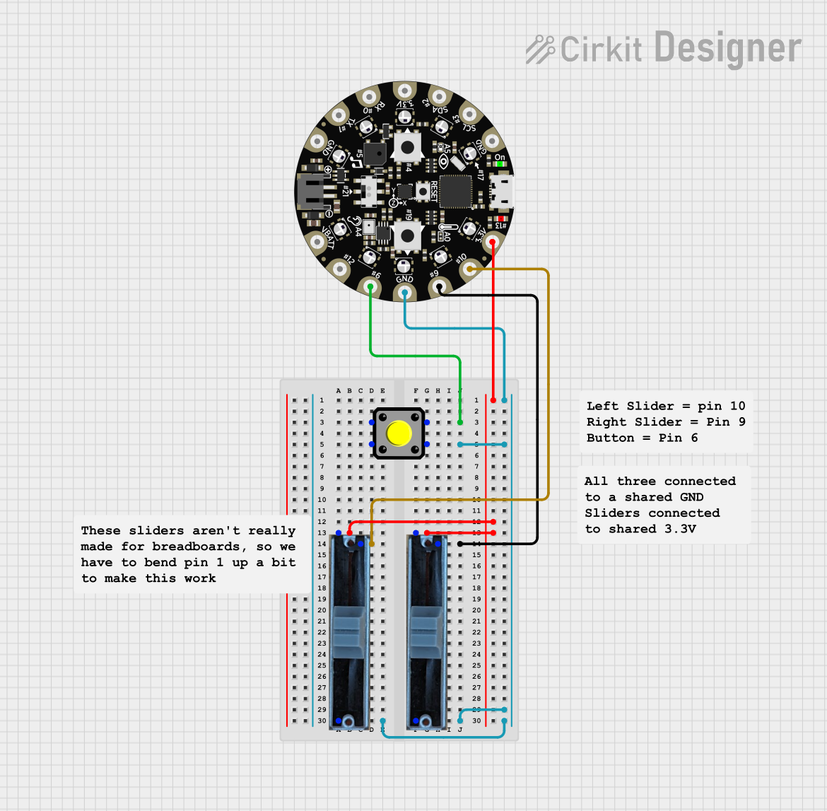
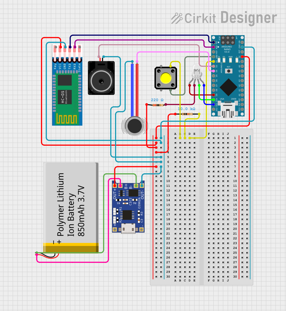
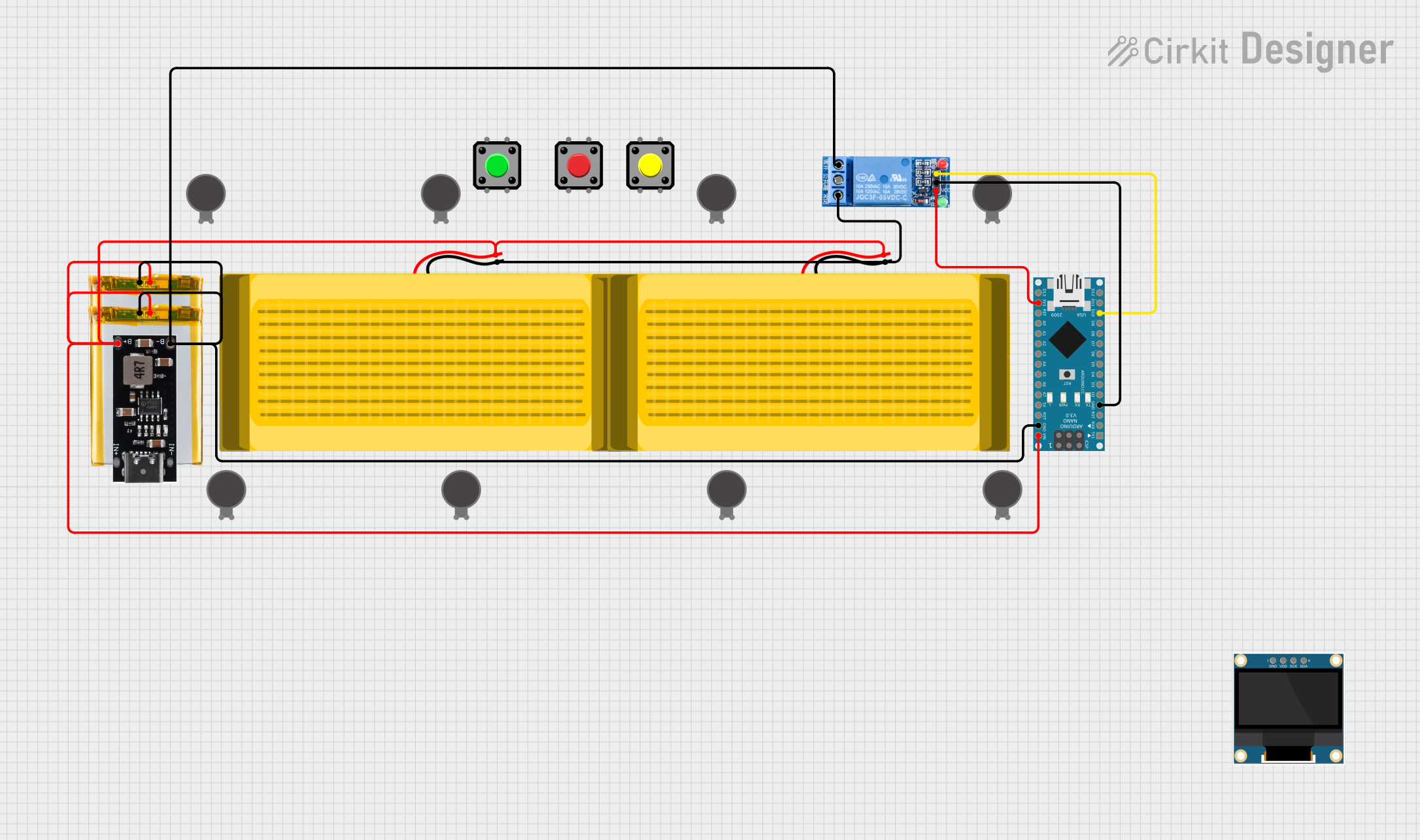
Explore Projects Built with PAD
Technical Specifications
PADs themselves do not have electrical ratings, as they are passive connection points. However, their design and material properties are critical for ensuring reliable electrical and mechanical connections. Below are the key technical details:
General Specifications
| Parameter | Description |
|---|---|
| Material | Typically copper, often plated with tin, gold, or other conductive coatings |
| Shape | Circular, rectangular, oval, or custom |
| Size | Varies based on PCB design; typically measured in mils (thousandths of an inch) |
| Surface Finish | HASL (Hot Air Solder Leveling), ENIG (Electroless Nickel Immersion Gold), etc. |
| Solderability | Designed to ensure strong and reliable solder joints |
| Thermal Resistance | Depends on PCB material and copper thickness |
Example Pin Configuration
While PADs do not have pins, they are often associated with specific PCB layers and functions. Below is an example of how PADs might be configured in a PCB design:
| Layer | Description |
|---|---|
| Top Layer | Used for surface-mount components or connections |
| Bottom Layer | Used for through-hole components or additional connections |
| Ground Plane | PADs may connect to the ground layer for grounding purposes |
| Signal Layer | PADs may connect to signal traces for data or power transmission |
Usage Instructions
How to Use PADs in a Circuit
Designing the PCB:
- Use PCB design software (e.g., KiCad, Eagle, or Altium Designer) to place PADs where components will be soldered.
- Ensure the PAD size and shape match the component leads or terminals.
- Assign appropriate net connections to each PAD (e.g., ground, power, or signal).
Soldering Components:
- Clean the PADs to remove any oxidation or contaminants.
- Apply solder paste (for surface-mount components) or flux (for through-hole components).
- Place the component leads onto the PADs and solder them using a soldering iron or reflow oven.
Testing and Debugging:
- Use PADs as test points to measure voltages, currents, or signals in the circuit.
- Ensure that the solder joints are clean and free of cold solder or bridging.
Important Considerations and Best Practices
- Thermal Relief: For PADs connected to large copper areas (e.g., ground planes), use thermal relief patterns to make soldering easier.
- Pad Size: Ensure the PAD size is appropriate for the component to avoid weak solder joints or mechanical stress.
- Surface Finish: Choose a surface finish that matches the application (e.g., ENIG for high-reliability circuits).
- Clearances: Maintain proper spacing between PADs to prevent short circuits or solder bridging.
Example: Connecting a PAD to an Arduino UNO
If a PAD is used as a connection point for an external wire to an Arduino UNO, you can solder a wire to the PAD and connect it to the Arduino's pin header. Below is an example Arduino code snippet for reading a signal from a PAD connected to pin A0:
// Example Arduino code to read an analog signal from a PAD connected to pin A0

void setup() {
  Serial.begin(9600); // Initialize serial communication at 9600 baud
  pinMode(A0, INPUT); // Set pin A0 as an input
}

void loop() {
  int sensorValue = analogRead(A0); // Read the analog value from the PAD
  Serial.print("Analog Value: ");
  Serial.println(sensorValue); // Print the value to the Serial Monitor
  delay(500); // Wait for 500 milliseconds before the next reading
}
Troubleshooting and FAQs
Common Issues
Poor Solder Joints:
- Cause: Oxidation on the PAD surface or insufficient solder.
- Solution: Clean the PAD with isopropyl alcohol and apply flux before soldering.
Solder Bridging:
- Cause: Excess solder or PADs placed too close together.
- Solution: Use a solder wick or desoldering pump to remove excess solder. Redesign the PCB with proper clearances if necessary.
PAD Lifting:
- Cause: Excessive heat during soldering or mechanical stress.
- Solution: Use a temperature-controlled soldering iron and avoid applying excessive force to the PAD.
Signal Integrity Issues:
- Cause: Poor connection between the PAD and the trace or component.
- Solution: Ensure proper soldering and verify the PCB design for continuity.
FAQs
Q: Can PADs be used for high-current applications?
A: Yes, but the PAD size, copper thickness, and trace width must be designed to handle the current without overheating.
Q: What is the difference between a PAD and a via?
A: A PAD is a connection point for components, while a via is used to connect traces between different PCB layers.
Q: How do I prevent PAD oxidation?
A: Use a surface finish like ENIG or HASL, and store PCBs in a dry, controlled environment.
Q: Can I repair a damaged PAD?
A: Yes, you can use a PCB repair kit to replace or rebuild a damaged PAD, but it requires precision and care.