How to Use 74HC02: Examples, Pinouts, and Specs

Introduction
The 74HC02 is a logic chip that contains four independent 2-input NOR gates. It is part of the 74HC family of high-speed CMOS devices. NOR gates are a fundamental component in digital electronics, providing a logical operation that outputs a HIGH signal only when all inputs are LOW. This makes the 74HC02 versatile for creating various logic circuits, including inverters, oscillators, and complex logic networks.
Common applications of the 74HC02 include:
- Digital logic circuits
- Signal processing
- Control systems
- Function generators
- Computer logic components
Explore Projects Built with 74HC02
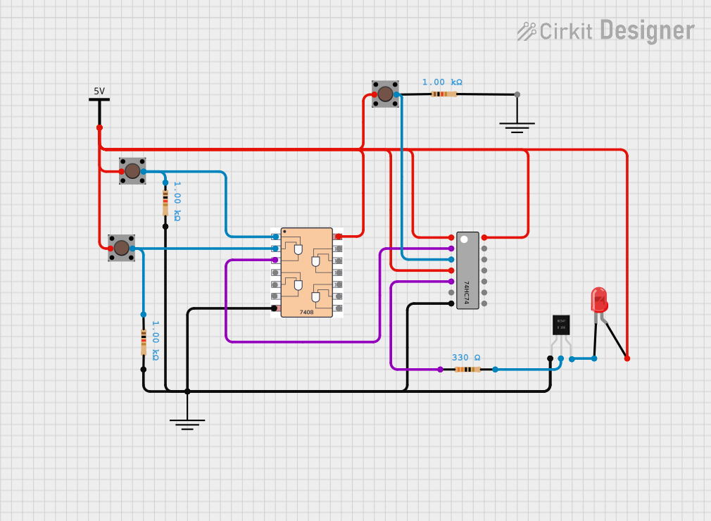
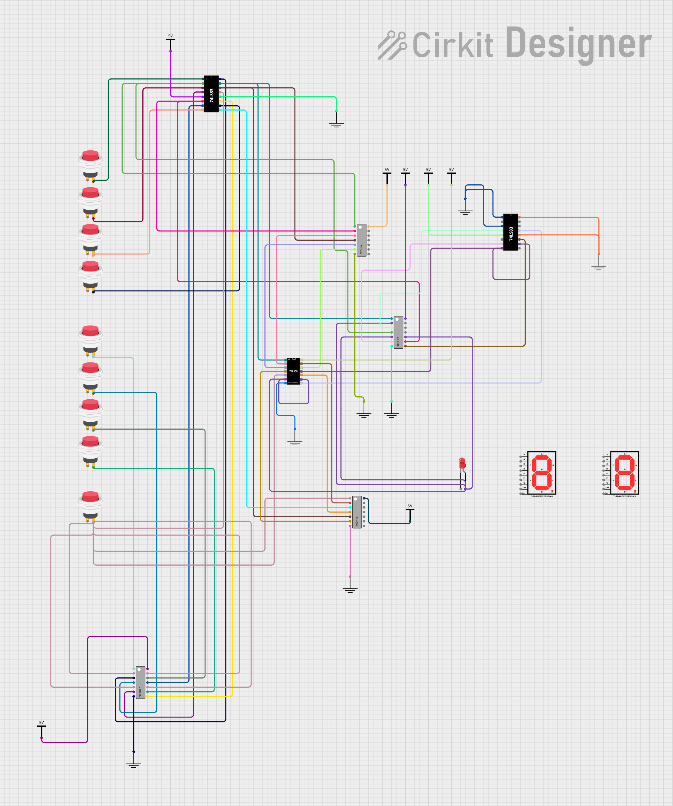
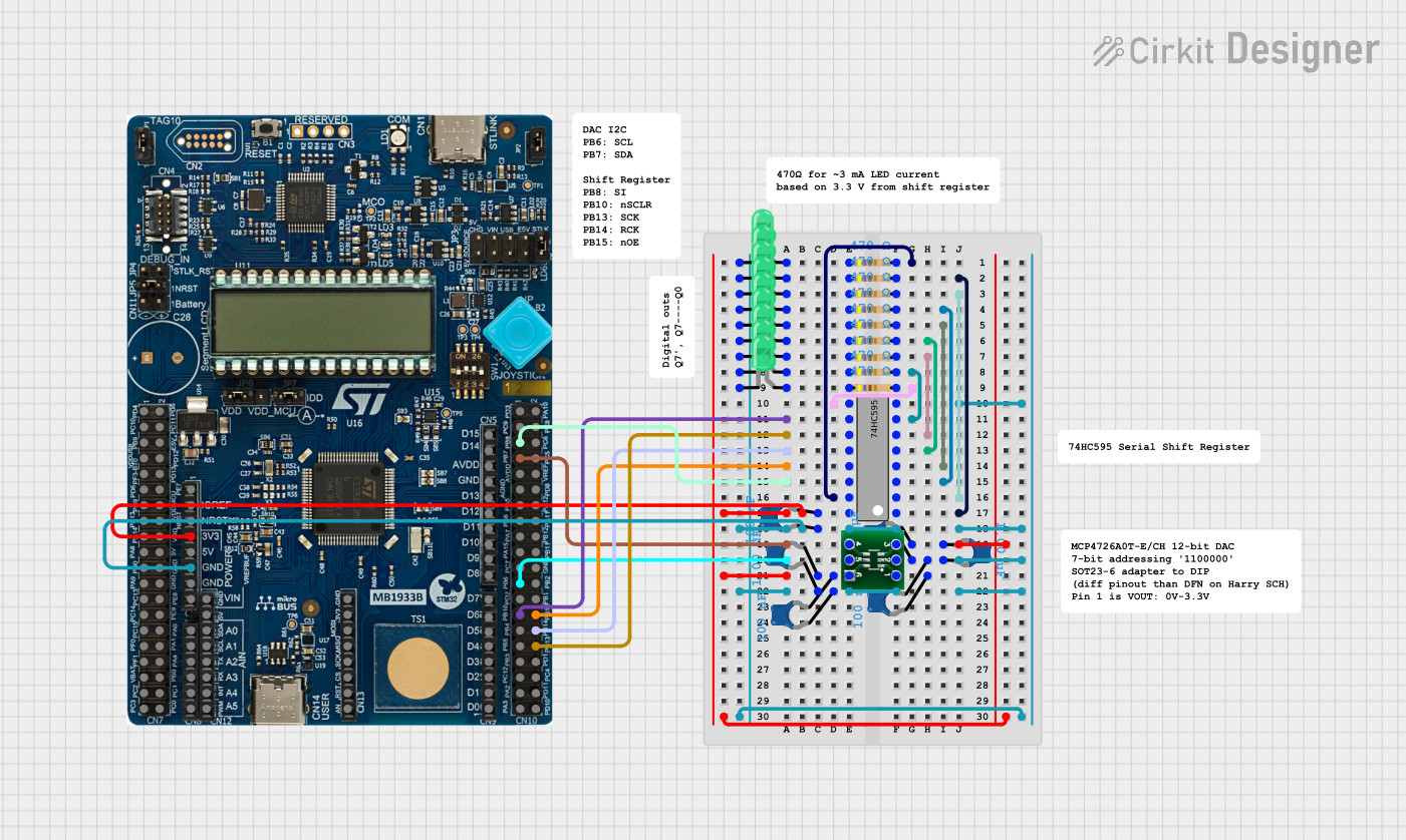
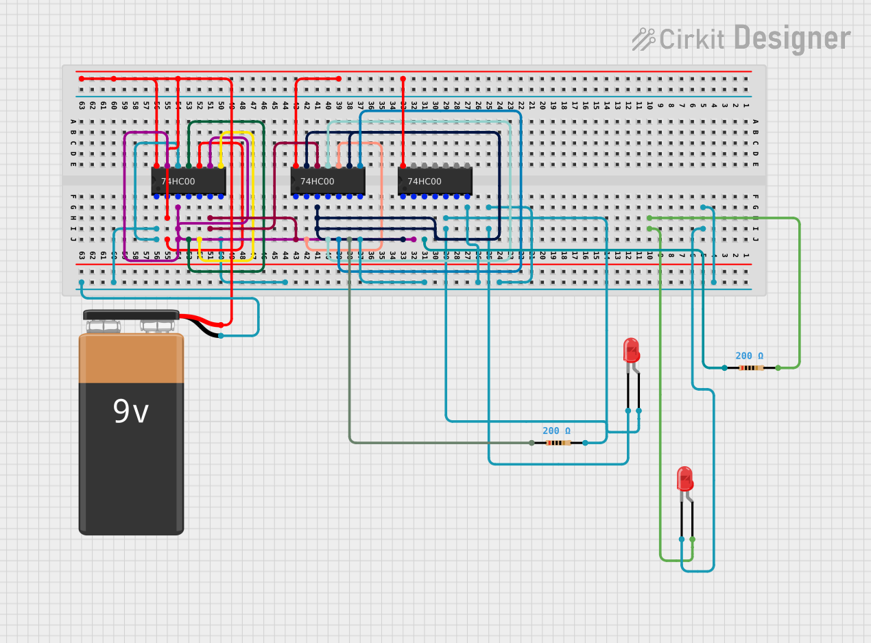
Explore Projects Built with 74HC02
Technical Specifications
Key Technical Details
- Supply Voltage (Vcc): 2.0V to 6.0V
- Input Voltage (Vin): 0V to Vcc
- Output Voltage (Vout): 0V to Vcc
- High-Level Input Voltage (VIH): Minimum 2.0V
- Low-Level Input Voltage (VIL): Maximum 0.8V
- High-Level Output Current (IOH): -5.2 mA (max)
- Low-Level Output Current (IOL): 5.2 mA (max)
- Propagation Delay Time: Varies with Vcc, input type, and temperature
- Operating Temperature Range: -40°C to +125°C
Pin Configuration and Descriptions
| Pin Number | Name | Description |
|---|---|---|
| 1 | 1A | Input A for Gate 1 |
| 2 | 1B | Input B for Gate 1 |
| 3 | 1Y | Output for Gate 1 |
| 4 | 2Y | Output for Gate 2 |
| 5 | 2A | Input A for Gate 2 |
| 6 | 2B | Input B for Gate 2 |
| 7 | GND | Ground (0V) |
| 8 | 3A | Input A for Gate 3 |
| 9 | 3B | Input B for Gate 3 |
| 10 | 3Y | Output for Gate 3 |
| 11 | 4Y | Output for Gate 4 |
| 12 | 4A | Input A for Gate 4 |
| 13 | 4B | Input B for Gate 4 |
| 14 | Vcc | Positive Supply Voltage |
Usage Instructions
How to Use the 74HC02 in a Circuit
- Connect the Vcc pin to a positive supply voltage within the range of 2.0V to 6.0V.
- Connect the GND pin to the ground of the power supply.
- Apply input signals to the A and B inputs of the desired NOR gate(s).
- The output Y of each gate will be HIGH only if both inputs A and B are LOW.
Important Considerations and Best Practices
- Ensure that the supply voltage does not exceed the maximum rating to prevent damage.
- Inputs should not be left floating; they should be connected to Vcc or GND if unused.
- Use pull-up or pull-down resistors if necessary to maintain a defined logic level when inputs are not driven.
- Decoupling capacitors (typically 0.1 µF) should be placed close to the Vcc pin to filter out noise.
Troubleshooting and FAQs
Common Issues
- Outputs not behaving as expected: Verify that all inputs are connected correctly and that the supply voltage is within the specified range.
- Device heating up: Check for short circuits or supply voltage exceeding the maximum rating.
Solutions and Tips
- Double-check wiring and ensure that the chip is oriented correctly in the circuit.
- Use a multimeter to measure the supply voltage and verify that it is within the recommended range.
- If the chip is not functioning, replace it with a new one to rule out the possibility of a defective component.
FAQs
Q: Can the 74HC02 be used with TTL logic levels? A: Yes, the 74HC02 is compatible with TTL logic levels when operated within the appropriate voltage range.
Q: What happens if the inputs are left floating? A: Floating inputs can pick up noise and result in unpredictable output. It is best to tie unused inputs to a known logic level.
Q: Is it possible to create an inverter with the 74HC02? A: Yes, by connecting both inputs of a NOR gate together, you can create an inverter.
Example Code for Arduino UNO
The following example demonstrates how to use one of the NOR gates on the 74HC02 with an Arduino UNO to create a simple inverter circuit.
// Define the input and output pins
const int inputPin = 2;  // Connect to 1A and 1B on the 74HC02
const int outputPin = 3; // Connect to 1Y on the 74HC02

void setup() {
  pinMode(inputPin, OUTPUT);
  pinMode(outputPin, INPUT);
}

void loop() {
  // Set the input to HIGH
  digitalWrite(inputPin, HIGH);
  // Read the output, which should be LOW (inverted)
  bool invertedSignal = digitalRead(outputPin);
  // Delay for a bit before changing the input
  delay(500);

  // Set the input to LOW
  digitalWrite(inputPin, LOW);
  // Read the output, which should be HIGH (inverted)
  invertedSignal = digitalRead(outputPin);
  // Delay for a bit before changing the input
  delay(500);
}
Remember to connect the Vcc and GND pins of the 74HC02 to the 5V and GND pins on the Arduino, respectively. The code above toggles the input pin and reads the inverted output from the NOR gate configured as an inverter.