How to Use AFE7444EVM: Examples, Pinouts, and Specs
Introduction
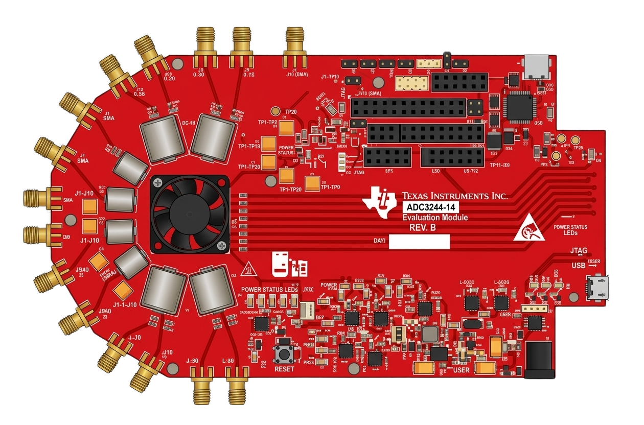
The AFE7444EVM is an evaluation module developed by Texas Instruments for the AFE7444, a high-performance analog front-end (AFE) designed for multi-channel data acquisition systems. This module provides a platform to evaluate the capabilities of the AFE7444, which integrates signal conditioning, analog-to-digital conversion (ADC), and digital-to-analog conversion (DAC) functionalities.
The AFE7444EVM is ideal for applications requiring high-speed data acquisition and processing, such as:
- Wireless communication systems
- Medical imaging equipment
- Industrial automation and control systems
- Automotive radar and LiDAR systems
This evaluation module simplifies the testing and prototyping of the AFE7444, enabling engineers to accelerate the development of their designs.
Explore Projects Built with AFE7444EVM
Explore Projects Built with AFE7444EVM
Technical Specifications
Key Technical Details
| Parameter | Specification |
|---|---|
| Input Voltage Range | 5V DC (via external power supply or USB) |
| ADC Resolution | 14-bit |
| DAC Resolution | 14-bit |
| Sampling Rate | Up to 9 GSPS (DAC), Up to 3 GSPS (ADC) |
| Number of Channels | 4 Transmit (TX), 4 Receive (RX) |
| Communication Interface | JESD204B/C |
| Clocking | Integrated PLL with external clock input support |
| Operating Temperature Range | -40°C to +85°C |
| Dimensions | 120 mm x 120 mm |
Pin Configuration and Descriptions
The AFE7444EVM features multiple connectors and headers for interfacing with external systems. Below is a summary of the key connectors:
Power and Clock Inputs
| Pin/Connector Name | Description |
|---|---|
| J1 | 5V DC power input |
| J2 | External clock input for PLL |
Data Interfaces
| Pin/Connector Name | Description |
|---|---|
| J3 | JESD204B/C high-speed serial data interface |
| J4 | GPIO header for control and status signals |
RF Inputs and Outputs
| Pin/Connector Name | Description |
|---|---|
| RX1_IN, RX2_IN | RF input channels for ADC |
| TX1_OUT, TX2_OUT | RF output channels for DAC |
Usage Instructions
How to Use the AFE7444EVM in a Circuit
Powering the Module:
- Connect a 5V DC power supply to the J1 connector.
- Ensure the power supply can provide at least 2A of current for stable operation.
Clock Configuration:
- Use the onboard PLL for clock generation or connect an external clock source to J2.
- Configure the clock frequency according to the desired sampling rate.
Data Communication:
- Connect the JESD204B/C interface (J3) to a compatible FPGA or processor for data transfer.
- Use the GPIO header (J4) for additional control signals if required.
RF Signal Connections:
- Connect the RF input signals to RX1_IN and RX2_IN for ADC evaluation.
- Connect the RF output signals from TX1_OUT and TX2_OUT to an oscilloscope or other measurement equipment for DAC evaluation.
Software Configuration:
- Install the Texas Instruments GUI software for the AFE7444EVM on your PC.
- Use the GUI to configure the AFE7444 settings, such as channel selection, gain, and sampling rate.
Important Considerations and Best Practices
- Ensure proper grounding to minimize noise and interference.
- Use high-quality RF cables and connectors for accurate signal transmission.
- Avoid exceeding the specified input voltage range to prevent damage to the module.
- Follow the recommended operating temperature range for reliable performance.
Example: Interfacing with an FPGA
Below is an example of how to configure the AFE7444EVM with an FPGA for data acquisition:
// Example Verilog code for interfacing with the AFE7444EVM
// This code configures the JESD204B interface for data transfer

module afe7444_interface (
    input wire clk,          // System clock
    input wire reset_n,      // Active-low reset
    output wire jesd_tx,     // JESD204B transmit signal
    input wire jesd_rx       // JESD204B receive signal
);

// Instantiate JESD204B IP core
jesd204b_core jesd_inst (
    .clk(clk),
    .reset_n(reset_n),
    .tx(jesd_tx),
    .rx(jesd_rx)
);

// Additional logic for data processing can be added here

endmodule
Troubleshooting and FAQs
Common Issues and Solutions
No Power to the Module:
- Issue: The module does not power on.
- Solution: Verify the power supply connection to J1 and ensure it provides 5V DC with sufficient current.
Clock Configuration Errors:
- Issue: The module does not generate or lock to the desired clock frequency.
- Solution: Check the external clock source connection to J2. Ensure the clock frequency matches the module's requirements.
Data Communication Failure:
- Issue: No data is transmitted or received via the JESD204B interface.
- Solution: Verify the FPGA configuration and ensure the JESD204B settings match the AFE7444EVM's configuration.
RF Signal Distortion:
- Issue: Output signals are distorted or noisy.
- Solution: Check the quality of the RF cables and connectors. Ensure proper grounding and shielding.
Frequently Asked Questions
Can the AFE7444EVM operate without an external clock?
- Yes, the module includes an onboard PLL that can generate the required clock signals.
What software is required to configure the AFE7444EVM?
- The Texas Instruments GUI software for the AFE7444EVM is required. It can be downloaded from the Texas Instruments website.
Is the AFE7444EVM compatible with all FPGAs?
- The module is compatible with FPGAs that support the JESD204B/C interface. Ensure the FPGA has sufficient resources for high-speed data processing.
What is the maximum sampling rate supported by the ADC and DAC?
- The ADC supports up to 3 GSPS, and the DAC supports up to 9 GSPS.
This documentation provides a comprehensive guide to understanding and using the AFE7444EVM. For further details, refer to the official Texas Instruments datasheet and user guide.