How to Use PCF8574: Examples, Pinouts, and Specs
Introduction
The PCF8574 is an I2C I/O expander that provides 8 additional general-purpose input/output (GPIO) pins. It is designed to interface with microcontrollers via the I2C protocol, enabling the expansion of GPIO capabilities without requiring additional microcontroller pins. This makes it an excellent choice for projects that require more I/O pins than are available on the microcontroller.
Explore Projects Built with PCF8574
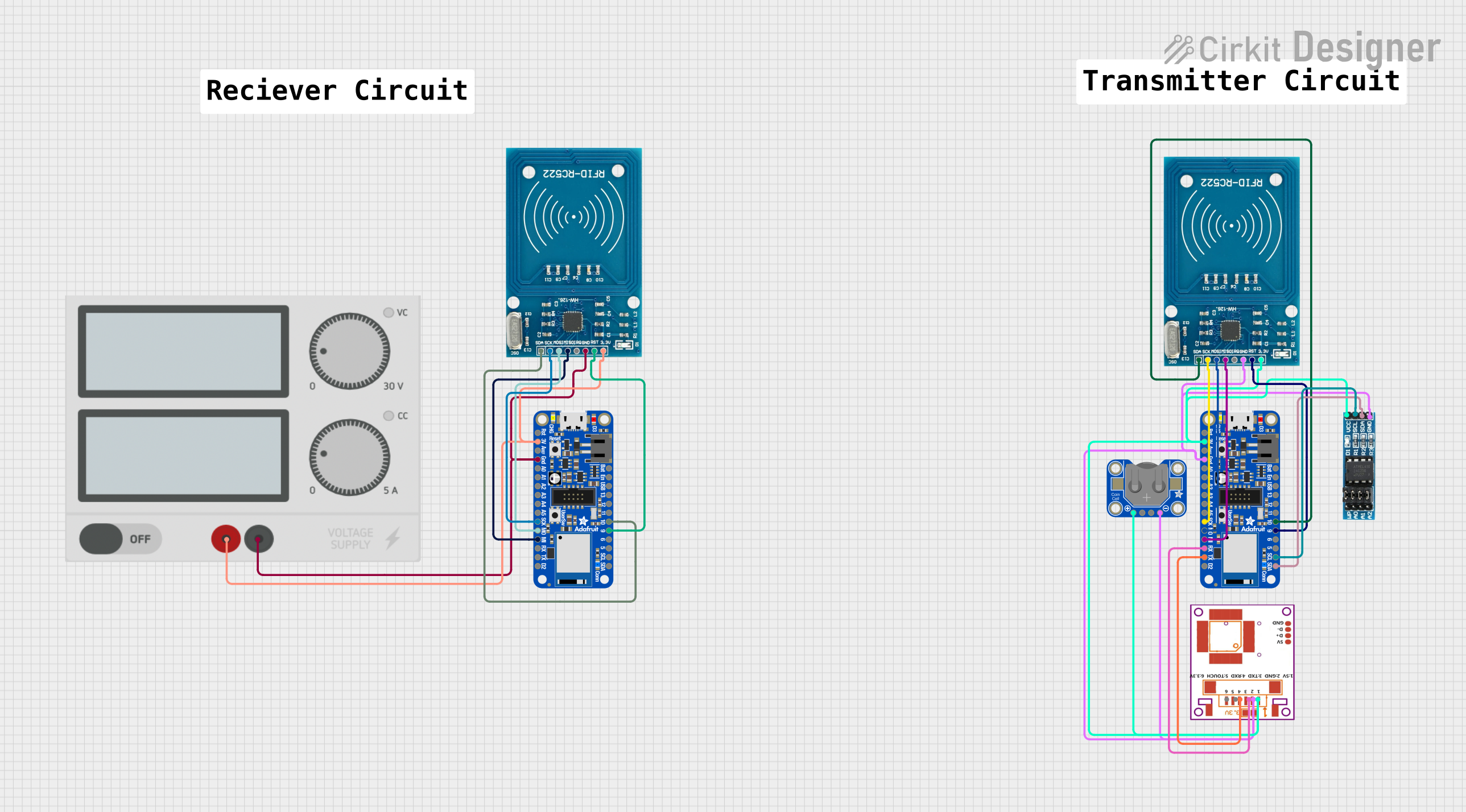
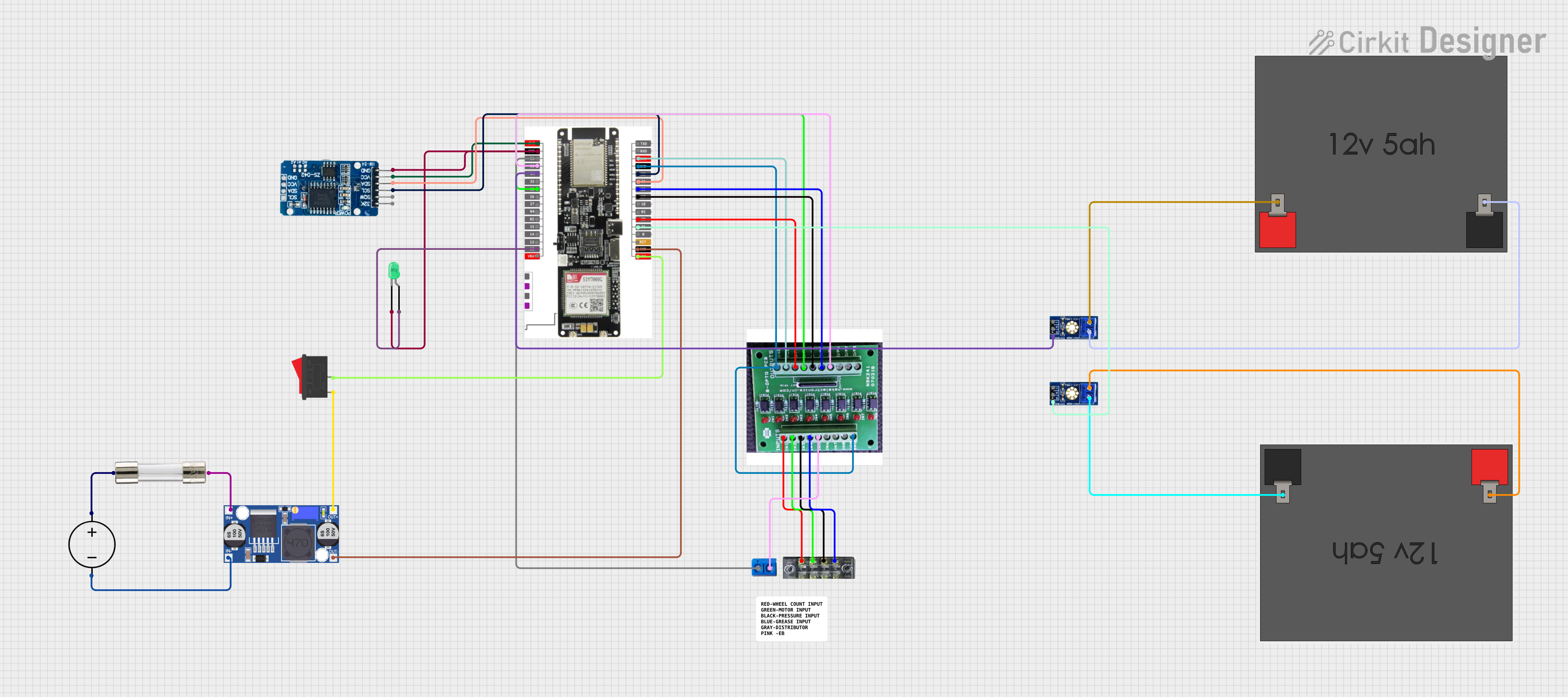
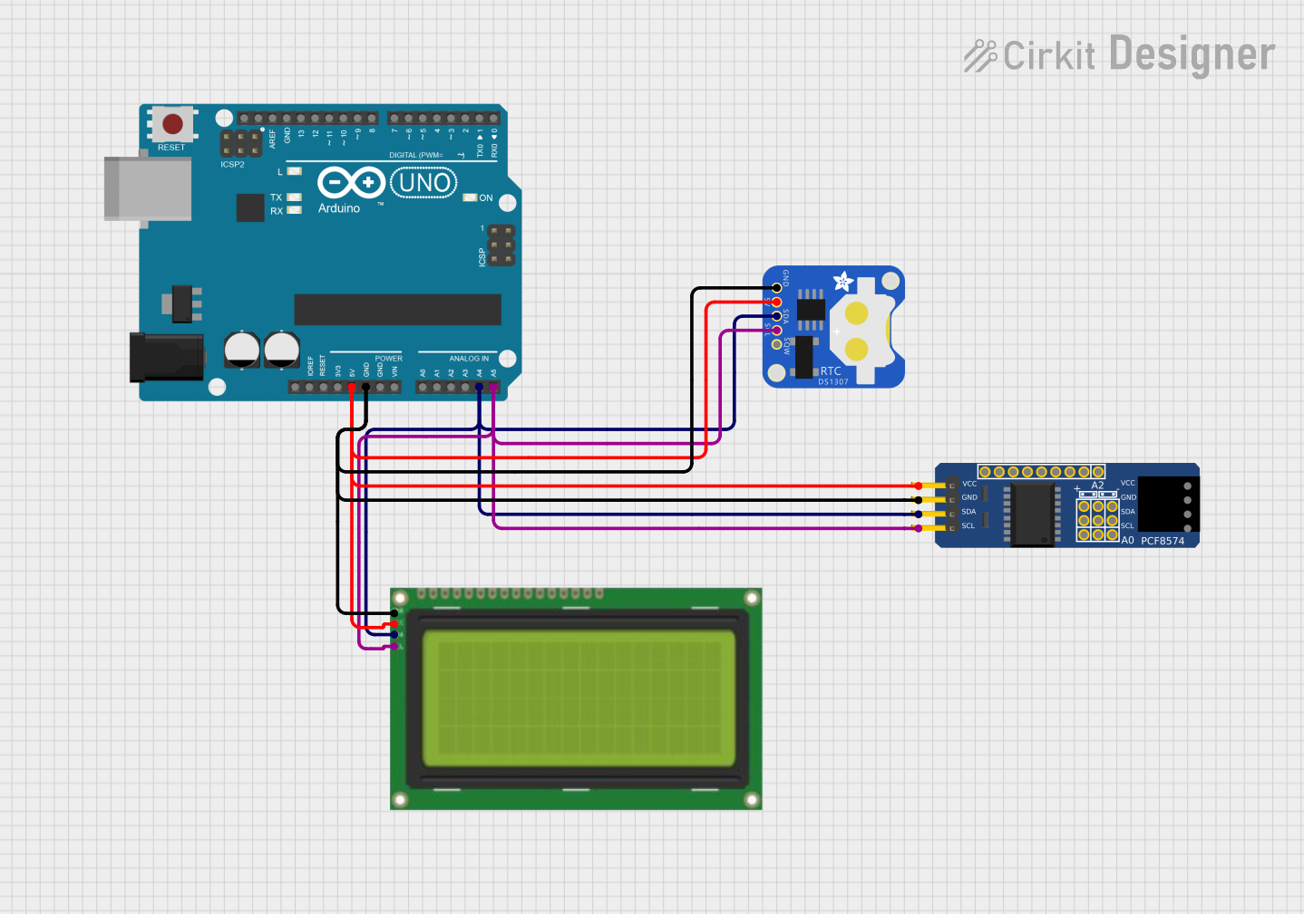
Explore Projects Built with PCF8574
Common Applications and Use Cases
- Expanding GPIO pins for microcontrollers in resource-constrained systems
- Interfacing with sensors, displays, and other peripherals
- Controlling LEDs, relays, or other output devices
- Reading input from buttons, switches, or other digital sensors
- Applications in home automation, robotics, and industrial control systems
Technical Specifications
The PCF8574 is a versatile and efficient I/O expander with the following key specifications:
| Parameter | Value |
|---|---|
| Operating Voltage | 2.5V to 6V |
| I2C Address Range | 0x20 to 0x27 (configurable via address pins) |
| Number of I/O Pins | 8 |
| Maximum Sink Current | 25 mA per pin |
| Maximum Source Current | 300 µA per pin |
| Communication Protocol | I2C (2-wire) |
| Operating Temperature | -40°C to +85°C |
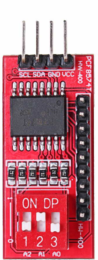
Pin Configuration and Descriptions
The PCF8574 comes in an 8-pin or 16-pin package, depending on the variant. Below is the pinout for the standard 16-pin DIP package:
| Pin | Name | Description |
|---|---|---|
| 1 | A0 | Address selection bit 0 (used to set the I2C address) |
| 2 | A1 | Address selection bit 1 (used to set the I2C address) |
| 3 | A2 | Address selection bit 2 (used to set the I2C address) |
| 4 | P0 | GPIO pin 0 (can be used as input or output) |
| 5 | P1 | GPIO pin 1 (can be used as input or output) |
| 6 | P2 | GPIO pin 2 (can be used as input or output) |
| 7 | P3 | GPIO pin 3 (can be used as input or output) |
| 8 | GND | Ground (0V reference) |
| 9 | P4 | GPIO pin 4 (can be used as input or output) |
| 10 | P5 | GPIO pin 5 (can be used as input or output) |
| 11 | P6 | GPIO pin 6 (can be used as input or output) |
| 12 | P7 | GPIO pin 7 (can be used as input or output) |
| 13 | INT | Interrupt output (active low, triggered by input state change) |
| 14 | SCL | I2C clock line |
| 15 | SDA | I2C data line |
| 16 | VCC | Power supply (2.5V to 6V) |
Usage Instructions
How to Use the PCF8574 in a Circuit
- Connect Power and Ground: Connect the
VCCpin to a 3.3V or 5V power supply and theGNDpin to ground. - Set the I2C Address: Configure the I2C address by connecting the
A0,A1, andA2pins to eitherVCC(logic HIGH) orGND(logic LOW). This allows up to 8 PCF8574 devices to be used on the same I2C bus. - Connect the I2C Lines: Connect the
SCLandSDApins to the corresponding I2C lines on the microcontroller. Use pull-up resistors (typically 4.7kΩ) on both lines if not already present. - Connect GPIO Devices: Attach the devices you want to control or monitor to the GPIO pins (
P0toP7). Configure each pin as input or output in your code.
Important Considerations and Best Practices
- Pull-up Resistors: Ensure proper pull-up resistors are used on the I2C lines (
SCLandSDA) to maintain signal integrity. - Interrupt Pin: Use the
INTpin to detect changes in input states without continuously polling the device. - Current Limitations: Be mindful of the current limitations for each GPIO pin (25 mA sink, 300 µA source). Use external transistors or relays for higher current loads.
- Address Conflicts: Avoid I2C address conflicts when using multiple devices on the same bus.
Example Code for Arduino UNO
Below is an example of how to use the PCF8574 with an Arduino UNO to toggle an LED connected to GPIO pin P0:
#include <Wire.h> // Include the Wire library for I2C communication

#define PCF8574_ADDRESS 0x20 // Default I2C address of the PCF8574

void setup() {
  Wire.begin(); // Initialize I2C communication
  Serial.begin(9600); // Initialize serial communication for debugging

  // Set all GPIO pins to HIGH (default state)
  Wire.beginTransmission(PCF8574_ADDRESS);
  Wire.write(0xFF); // All pins HIGH
  Wire.endTransmission();

  Serial.println("PCF8574 initialized.");
}

void loop() {
  // Toggle GPIO pin P0 (connected to an LED)
  Wire.beginTransmission(PCF8574_ADDRESS);
  Wire.write(0xFE); // Set P0 LOW, others HIGH
  Wire.endTransmission();
  delay(500); // Wait for 500ms

  Wire.beginTransmission(PCF8574_ADDRESS);
  Wire.write(0xFF); // Set all pins HIGH
  Wire.endTransmission();
  delay(500); // Wait for 500ms
}
Troubleshooting and FAQs
Common Issues and Solutions
I2C Communication Failure
- Cause: Incorrect wiring or missing pull-up resistors on
SCLandSDA. - Solution: Verify connections and ensure 4.7kΩ pull-up resistors are present.
- Cause: Incorrect wiring or missing pull-up resistors on
GPIO Pins Not Responding
- Cause: Incorrect I2C address or pin configuration.
- Solution: Double-check the I2C address and ensure the pins are configured correctly in the code.
Interrupt Pin Not Working
- Cause: Interrupt pin not connected or not enabled in the code.
- Solution: Connect the
INTpin to a microcontroller interrupt-capable pin and configure it in the code.
Overcurrent on GPIO Pins
- Cause: Exceeding the current limits of the GPIO pins.
- Solution: Use external transistors or relays for high-current loads.
FAQs
Can the PCF8574 be used with 3.3V microcontrollers?
- Yes, the PCF8574 operates at 2.5V to 6V, making it compatible with both 3.3V and 5V systems.
How many PCF8574 devices can be connected to the same I2C bus?
- Up to 8 devices can be connected by configuring the
A0,A1, andA2address pins.
- Up to 8 devices can be connected by configuring the
Can the GPIO pins be used as analog inputs?
- No, the GPIO pins are digital-only and cannot read analog signals.
What is the purpose of the
INTpin?- The
INTpin is used to signal the microcontroller when an input state changes, reducing the need for continuous polling.
- The