How to Use CD4066: Examples, Pinouts, and Specs
Introduction
The CD4066 is a quad bilateral switch that allows for the control of both analog and digital signals. It consists of four independent switches, each capable of bidirectional signal flow when activated. This component is widely used in applications such as signal routing, audio switching, multiplexing, and digital logic circuits. Its ability to handle both analog and digital signals makes it a versatile choice for a variety of electronic designs.
Explore Projects Built with CD4066
Explore Projects Built with CD4066
Common Applications:
- Signal routing in audio and video systems
- Analog and digital multiplexing
- Logic signal switching
- Sample-and-hold circuits
- Test equipment and instrumentation
Technical Specifications
The CD4066 is designed to operate over a wide range of voltages and is compatible with both CMOS and TTL logic levels. Below are its key technical details:
Key Specifications:
- Supply Voltage (Vdd): 3V to 15V
- Control Voltage (Vcontrol): 0V to Vdd
- On-State Resistance (Ron): 80Ω (typical) at Vdd = 10V
- Maximum Signal Voltage: Vdd
- Maximum Signal Current: 10mA
- Power Dissipation: 700mW (maximum)
- Operating Temperature Range: -55°C to +125°C
- Switching Speed: 125ns (typical) at Vdd = 10V
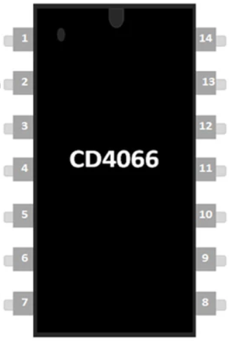
Pin Configuration and Descriptions:
The CD4066 is available in a 14-pin DIP (Dual Inline Package) or SOIC (Small Outline Integrated Circuit) package. Below is the pinout and description:
| Pin Number | Pin Name | Description |
|---|---|---|
| 1 | Control 1 | Control input for Switch 1 |
| 2 | Input/Output 1A | Input/Output terminal A for Switch 1 |
| 3 | Input/Output 1B | Input/Output terminal B for Switch 1 |
| 4 | Control 2 | Control input for Switch 2 |
| 5 | Input/Output 2A | Input/Output terminal A for Switch 2 |
| 6 | Input/Output 2B | Input/Output terminal B for Switch 2 |
| 7 | Vss | Ground (0V) |
| 8 | Input/Output 3B | Input/Output terminal B for Switch 3 |
| 9 | Input/Output 3A | Input/Output terminal A for Switch 3 |
| 10 | Control 3 | Control input for Switch 3 |
| 11 | Input/Output 4B | Input/Output terminal B for Switch 4 |
| 12 | Input/Output 4A | Input/Output terminal A for Switch 4 |
| 13 | Control 4 | Control input for Switch 4 |
| 14 | Vdd | Positive supply voltage |
Usage Instructions
The CD4066 can be used to switch signals by applying a control voltage to the respective control pin. When the control voltage is high (logic "1"), the corresponding switch is closed, allowing signals to pass between the two terminals (A and B). When the control voltage is low (logic "0"), the switch is open, and the signal is blocked.
Steps to Use the CD4066:
- Power the IC: Connect the Vdd pin to a positive voltage supply (3V to 15V) and the Vss pin to ground.
- Connect the Signal Terminals: Attach the signal source to one terminal (e.g., A) and the destination to the other terminal (e.g., B) of the desired switch.
- Control the Switch: Apply a control voltage to the corresponding control pin. A high voltage (close to Vdd) will close the switch, while a low voltage (close to Vss) will open it.
- Ensure Signal Compatibility: Ensure that the signal voltage does not exceed the supply voltage (Vdd) and that the current is within the specified limits.
Example Circuit with Arduino UNO:
The CD4066 can be controlled using an Arduino UNO to switch signals. Below is an example of how to control one of the switches:
Circuit Connections:
- Connect Vdd to the 5V pin of the Arduino.
- Connect Vss to the GND pin of the Arduino.
- Connect the control pin (e.g., Control 1) to a digital output pin of the Arduino (e.g., pin 7).
- Connect the signal source to Input/Output 1A and the destination to Input/Output 1B.
Arduino Code:
// CD4066 Control Example
// This code demonstrates how to control a switch on the CD4066 using an Arduino UNO.

const int controlPin = 7; // Pin connected to Control 1 of the CD4066

void setup() {
  pinMode(controlPin, OUTPUT); // Set the control pin as an output
}

void loop() {
  digitalWrite(controlPin, HIGH); // Close the switch (logic "1")
  delay(1000); // Keep the switch closed for 1 second

  digitalWrite(controlPin, LOW); // Open the switch (logic "0")
  delay(1000); // Keep the switch open for 1 second
}
Best Practices:
- Use decoupling capacitors (e.g., 0.1µF) near the Vdd pin to stabilize the power supply.
- Avoid exceeding the maximum voltage and current ratings to prevent damage to the IC.
- For analog signals, consider the on-state resistance (Ron) and its effect on signal quality.
Troubleshooting and FAQs
Common Issues:
Switch Not Activating:
- Ensure the control voltage is within the specified range (0V to Vdd).
- Check for loose or incorrect connections.
Signal Distortion:
- Verify that the signal voltage and current are within the IC's limits.
- Consider the on-state resistance (Ron) and its impact on high-frequency signals.
Excessive Heat:
- Ensure the total power dissipation does not exceed 700mW.
- Check for short circuits or excessive current through the switches.
FAQs:
Q: Can the CD4066 handle AC signals?
A: Yes, the CD4066 can handle AC signals as long as the peak voltage does not exceed the supply voltage (Vdd).
Q: What happens if the control pin is left floating?
A: A floating control pin may cause unpredictable behavior. Always tie unused control pins to a defined logic level (e.g., GND or Vdd).
Q: Can I use the CD4066 for high-frequency signals?
A: The CD4066 is suitable for low to moderate frequency signals. For high-frequency applications, consider the on-state resistance and parasitic capacitance, which may affect performance.
Q: Is the CD4066 compatible with 3.3V systems?
A: Yes, the CD4066 can operate at 3.3V, but ensure that the control and signal voltages do not exceed the supply voltage.